Electron beam apparatus and lens array

a technology of electron beam and lens array, which is applied in the direction of beam deviation/focusing by electric/magnetic means, instruments, mass spectrometers, etc., can solve the problems of difficult control of the curvature of field of the objective lens, the inability to easily change the diameter of the opening of the lens array, and the limited optical condition under which the curvature of field can be corrected

Inactive Publication Date: 2013-09-26
HITACHI HIGH-TECH CORP
View PDF3 Cites 60 Cited by
  • Summary
  • Abstract
  • Description
  • Claims
  • Application Information

AI Technical Summary

Benefits of technology

[0007]In the case of correcting the curvature of field aberration of an objective lens using, for example, the scheme disclosed in Japanese Unexamined Patent Application Publication No. 2007-123599, a likely problem will be that the diameter of the opening of the lens array cannot be easily changed, and therefore, an optical condition under which the curvature of field can be corrected will be restricted. More specifically, if a magnification of the objective lens is changed after once the lens array is installed in the apparatus, it will be difficult to control the curvature of field of the objective lens so as to match a change in the curvature of field aberration of the objective lens, accompanying a change in the magnification.

Problems solved by technology

In the case of correcting the curvature of field aberration of an objective lens using, for example, the scheme disclosed in Japanese Unexamined Patent Application Publication No. 2007-123599, a likely problem will be that the diameter of the opening of the lens array cannot be easily changed, and therefore, an optical condition under which the curvature of field can be corrected will be restricted.
More specifically, if a magnification of the objective lens is changed after once the lens array is installed in the apparatus, it will be difficult to control the curvature of field of the objective lens so as to match a change in the curvature of field aberration of the objective lens, accompanying a change in the magnification.
However, in reality, many technical problems are involved in preparing the lens array described in Japanese Unexamined Patent Application Publication No. 2001-267221.
Further, in consideration of many power supplies, and circuits, necessary in order to control voltages applied to the respective electron beams, it can be said that this method has a problem from a cost point of view, as well.

Method used


Image

  • Electron beam apparatus and lens array
  • Electron beam apparatus and lens array
  • Electron beam apparatus and lens array

Examples


first embodiment

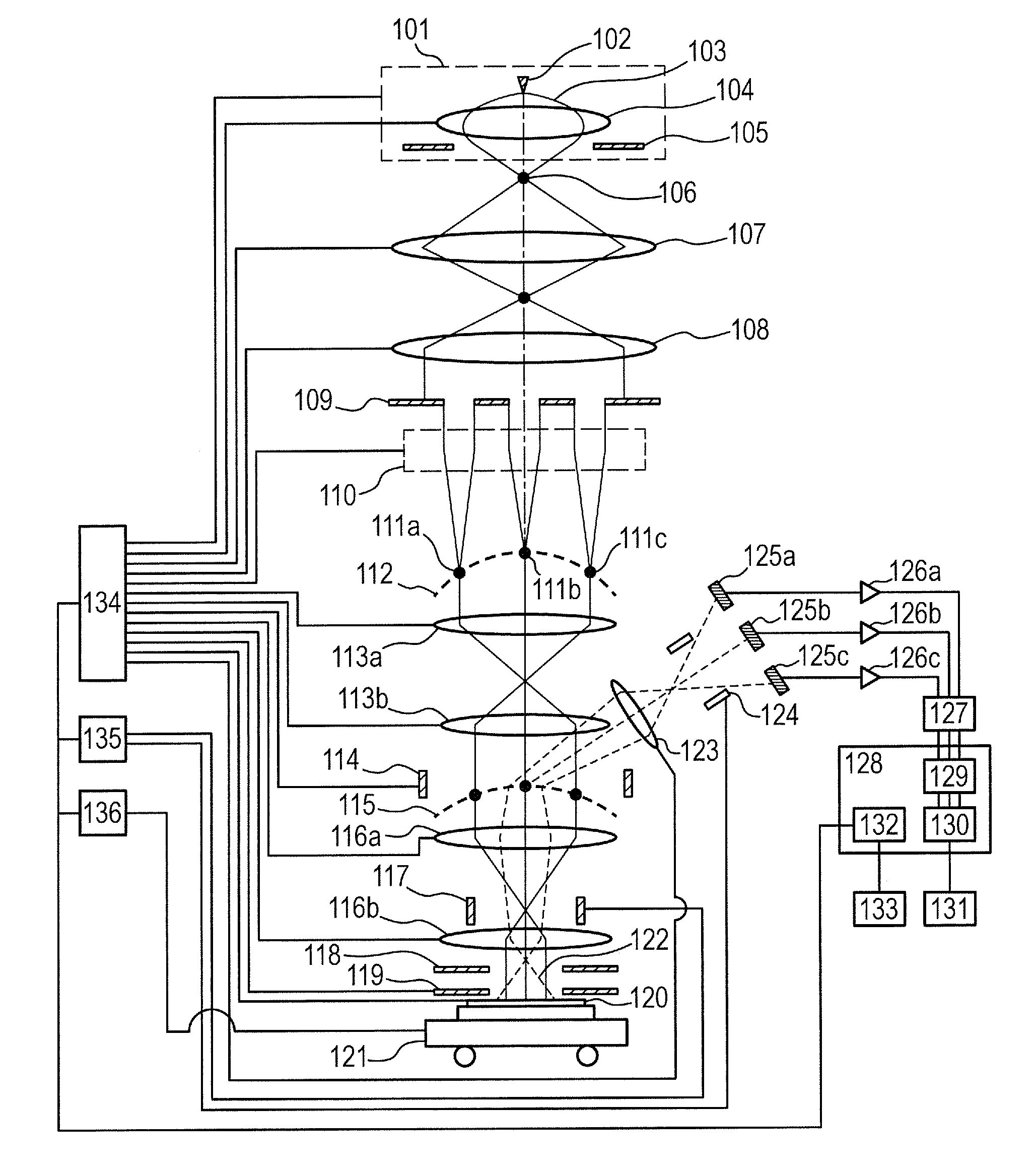
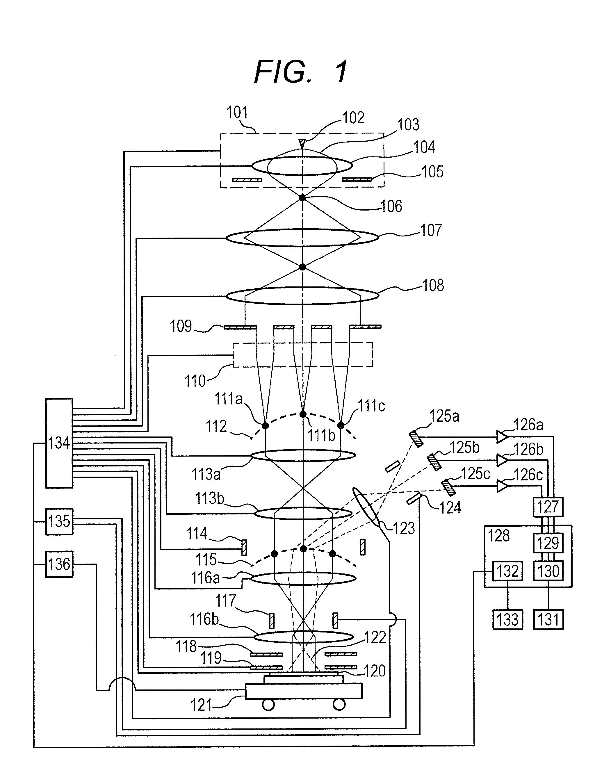
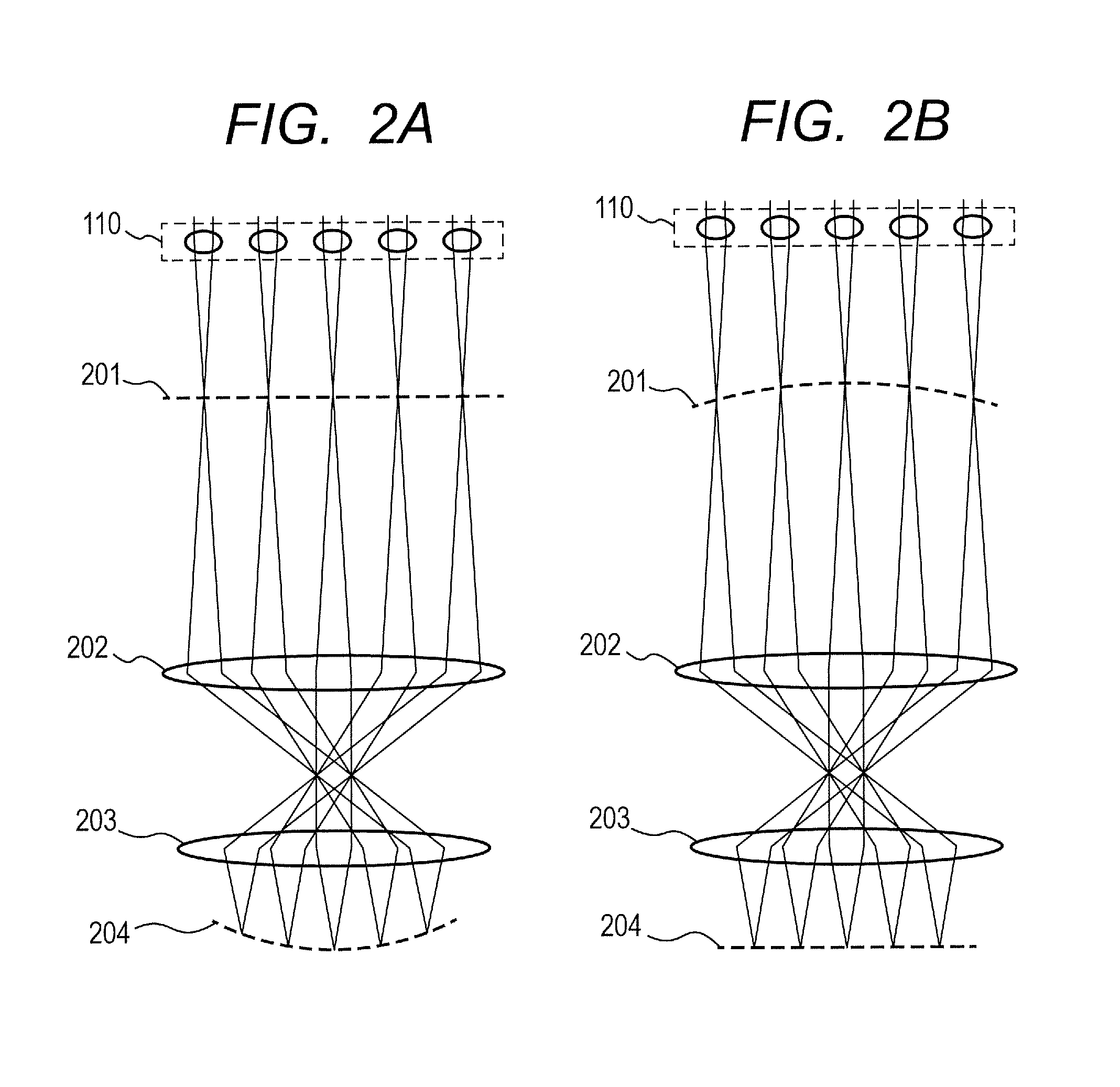
[0048]In a microscope for application to a semiconductor process, such as, for example, an electron beam inspection apparatus, an electron beam measuring apparatus, and so forth, the variety of controls as to an optical condition, according to a specimen, are required. Under such circumstances, a lens array according to the related art is unable to independently control an image forming position using a lens close to a center axis, and a curvature of a lens array image surface (a lens array image-forming surface or a crossover image surface), so that it has become difficult to have a desirable optical condition compatible with the correction of the curvature of field aberration. In the first embodiment of the invention, with an eye on this point, it is intended to implement an electron beam apparatus capable of independently controlling the image forming position by the lens close to the center axis, and the curvature of the lens array image surface. As one of specific unit (will be...

second embodiment

[0096]FIGS. 8A to 8C each are a schematic representation showing an example of the configuration of a lens array in an electron beam apparatus according to a second embodiment of the invention. The lens array shown in FIG. 8A is comprised of two units of lens arrays, including a first lens array 801, and a second lens array 805. The first lens array 801 is comprised of 3 plates of electrodes, including a first electrode 802, a second electrode 803, and a third electrode 804, provided in this order from the upstream side (a side of the lens array, adjacent to an electron gun). The respective electrodes have 25 pieces of openings formed therein. The respective openings are circular in shape, and the respective openings in each of the electrodes are disposed such that a beam axis of each of 25 lengths of beams, indicated by a solid line in the figure, penetrates through the center of the opening. A common voltage (in this case, the ground voltage) is connected to the first electrode 80...

third embodiment

[0101]FIG. 9A is a schematic representation showing an example of the configuration of a lens array in an electron beam apparatus according to a third embodiment of the invention. The lens array shown in FIG. 9A is comprised of 5 plates of electrodes, including a first electrode 901, a second electrode 902, a third electrode 903, a fourth electrode 904, and a fifth electrode 905, provided in this order from the upstream side (a side of the lens array, adjacent to an electron gun). The lens array of FIG. 9A is made up so as to be vertically symmetrical about the third electrode 903, and an interval between the first electrode 901 and the second electrode 902 is equal to an interval between the fourth electrode 904 and the fifth electrode 905. Further, an interval between the second electrode 902 and the third electrode 903 is equal to an interval between the third electrode 903 and the fourth electrode 904. Multiple openings, each thereof being circular in shape, are disposed in each...


PUM

PropertyMeasurementUnit
shapeaaaaaaaaaa
curvatureaaaaaaaaaa
voltagesaaaaaaaaaa

Abstract

There is provided both an electron beam apparatus and a lens array, capable of correcting a curvature of field aberration under various optical conditions. The electron beam apparatus comprises the lens array having a plurality of electrodes, and multiple openings are formed in the respective electrodes. An opening diameter distribution with respect to the respective opening diameters of the plural openings formed in the respective electrodes are individually set, and voltages applied to the respective electrodes are independently controlled to thereby independently adjust an image forming position of a reference beam, and a curvature of the lens array image surface.

Description

CLAIM OF PRIORITY[0001]The present application claims priority from Japanese patent application JP 2012-063816 filed on Mar. 21, 2012, the content of which is hereby incorporated by reference into this application.FIELD OF THE INVENTION[0002]The present invention relates to an electron beam application technology, and in particular, to an electron beam apparatus such as an inspection apparatus, a microscope, and so forth, used in a semiconductor process, and a lens array incorporated therein.BACKGROUND OF THE INVENTION[0003]In a semiconductor process, use is made of an electron microscope for irradiating an electron beam called a primary beam onto a specimen to thereby make an observation of a pattern, and a structure, formed on the specimen such as a wafer, and so forth from a signal of a secondary electron, a reflection electron, and so forth (hereinafter called a secondary beam), that is, to carry out observation, measurement, inspection, and suchlike. The electron beam apparatus...

Claims


Application Information

Patent Timeline
Patent Type & Authority Applications(United States)
IPC IPC(8): H01J37/10
CPCH01J37/10H01J37/153H01J2237/1534H01J2237/121H01J2237/1205
Inventor TANIMOTO, SAYAKAOHTA, HIROYASAKAKIBARA, MAKOTOENYAMA, MOMOYOTANIMOTO, KENJI
Owner HITACHI HIGH-TECH CORP
Why Eureka
Try Eureka