Semiconductor device

a technology of semiconductor devices and dielectric devices, which is applied in the direction of semiconductor/solid-state device details, electrical apparatus construction details, printed circuit non-printed electric components association, etc., can solve the problems of deterioration of power modules b>600/b>, inability to suppress pressure on insulating substrates, etc., to prevent the displacement of control terminals, and prevent the effect of dielectric strength decreas

Active Publication Date: 2013-09-26
FUJI ELECTRIC CO LTD
View PDF4 Cites 15 Cited by
  • Summary
  • Abstract
  • Description
  • Claims
  • Application Information

AI Technical Summary

Benefits of technology

[0033]According to the above aspect of the present invention, since the control terminal includes the protrusion portion and the L-shaped member, the protrusion portion and the L-shaped member of the control terminal are in contact with the front surface and the rear surface of the cover, respectively, so that the control terminal is fixed. Therefore, at the time of detaching the connector, a stress exerted on the control terminal is not transferred to the insulating substrate through the control terminal. Accordingly, at the time of detaching the connector, it is possible to prevent a decrease in dielectric strength due to fracture of the insulating substrate and to prevent displacement of the control terminal and damage to the solder attaching the control terminal and the insulating substrate due to depression of the insulating substrate.
[0034]In addition, according to the above aspect of the present invention, since the two protrusion portions interposing the cover of the resin case are installed in the portion of the control terminal which penetrates the case, the two protrusion portions are in contact with the front surface and the rear surface of the cover of the case, respectively, so that the control terminal is fixed. Therefore, at the time of detaching the connector, a stress exerted on the control terminal is not transferred to the insulating substrate through the control terminal. Accordingly, at the time of detaching the connector, it is possible to prevent a decrease in dielectric strength due to fracture of the insulating substrate and to prevent displacement of the control terminal and damage to the solder attaching the control terminal and the insulating substrate due to depression of the insulating substrate.
[0035]In addition, according to the above aspect of the present invention, since the notch portion is installed in the portion of the control terminal which penetrates the case, the upper sidewall and the lower sidewall of the notch portion are in contact with the front surface and the rear surface of the cover of the case, respectively, so that the control terminal is fixed. Therefore, at the time of detaching the connector, a stress exerted on the control terminal is not transferred to the insulating substrate through the control terminal. Accordingly, at the time of detaching the connector, it is possible to prevent a decrease in dielectric strength due to fracture of the insulating substrate and to prevent displacement of the control terminal and damage to the solder attaching the control terminal and the insulating substrate due to depression of the insulating substrate.
[0036]According to a semiconductor device of the present invention, it is possible to obtain an effect capable of providing a semiconductor device having high dielectric strength. In addition, according to a semiconductor device of the present invention, it is possible to obtain an effect capable of providing a semiconductor device having high reliability.

Problems solved by technology

Therefore, there is a problem in that the reliability of the power module 600 is deteriorated.
Therefore, in the case of attaching the connector to the control terminal, the pressure exerted on the insulating substrate cannot be suppressed.

Method used


Image

  • Semiconductor device
  • Semiconductor device
  • Semiconductor device

Examples


first embodiment

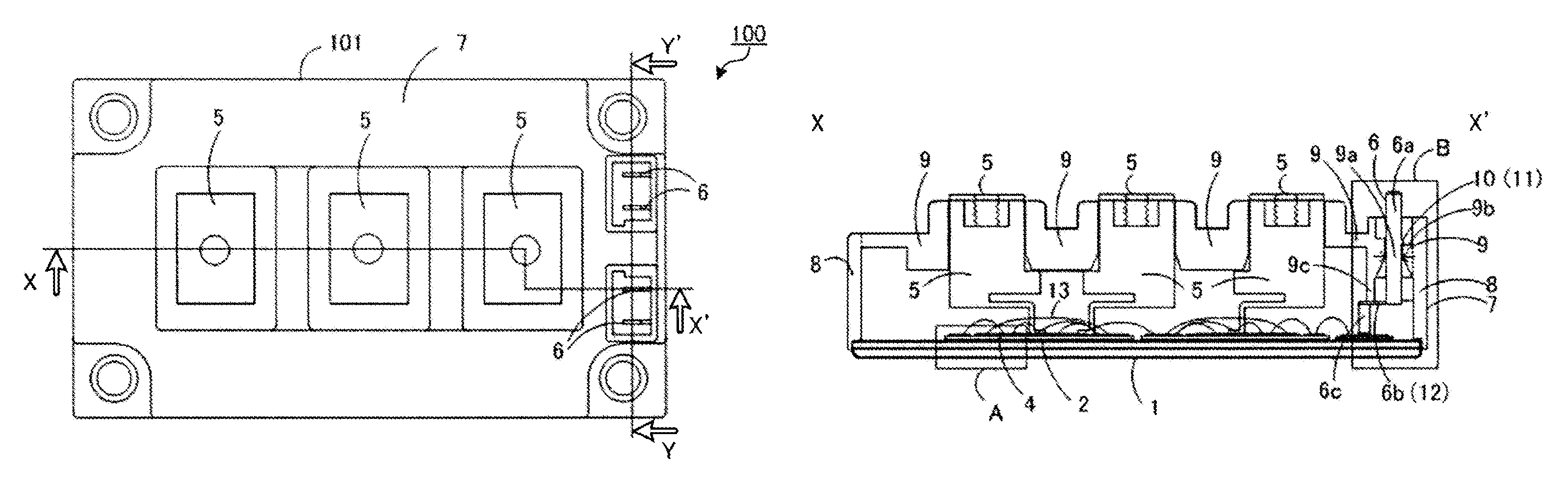
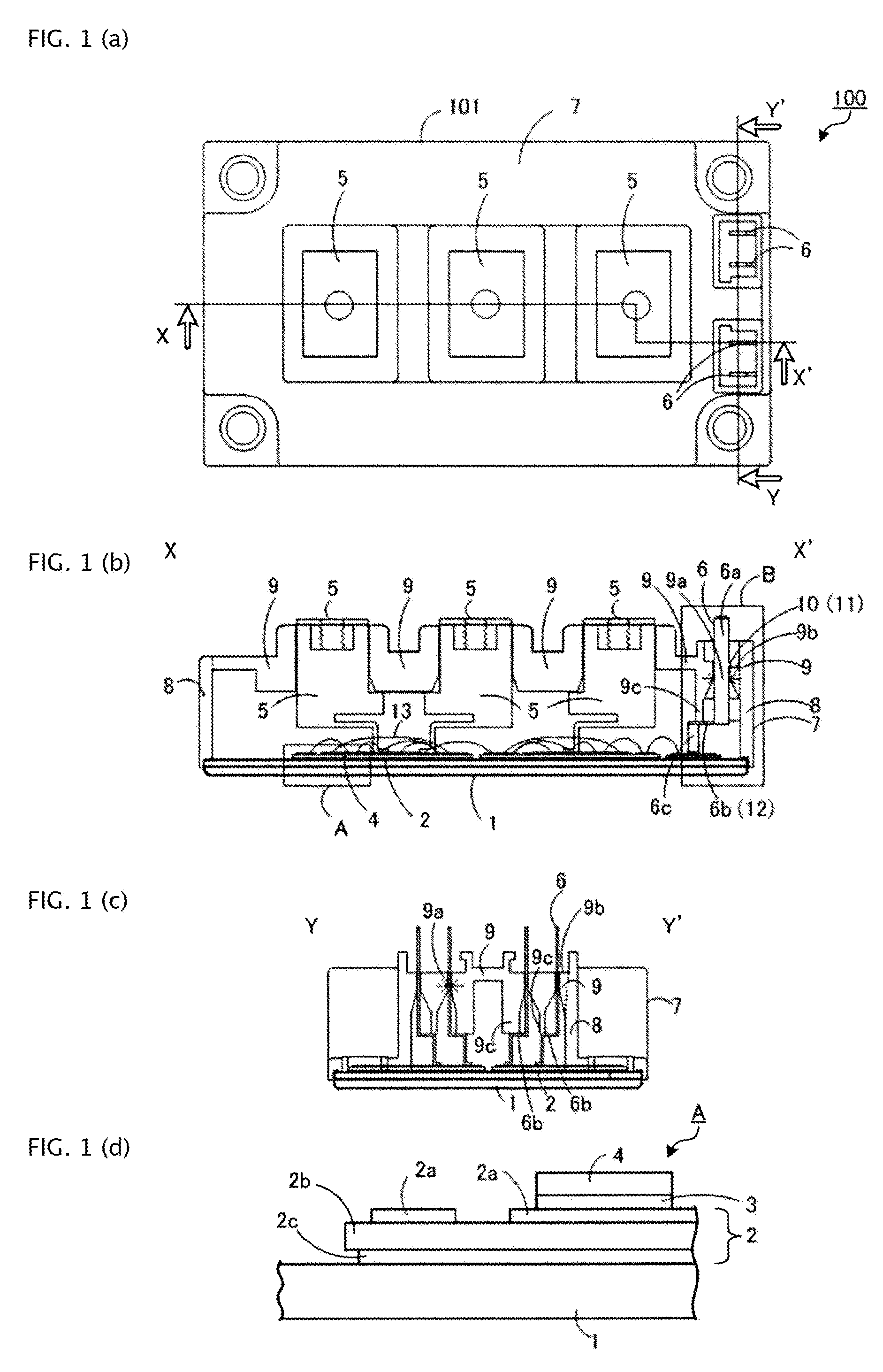
[0054]FIG. 1 is a diagram for describing a semiconductor device according to a first embodiment of the present invention. FIG. 1(a) illustrates a plan diagram of main components of a package 101 of a power module 100. FIG. 1(b) illustrates a cross-sectional diagram taken along line X-X′ in FIG. 1(a). FIG. 1(c) illustrates a cross-sectional diagram taken along line Y-Y′ in FIG. 1(a). FIGS. 1(b) and 1(c) illustrate the power module 100 seen in the direction of a white arrow illustrated in the vicinity of the cut line in FIG. 1(a). FIG. 1(d) illustrates enlargement of a vicinity A of an insulating substrate 2 of FIG. 1(b).

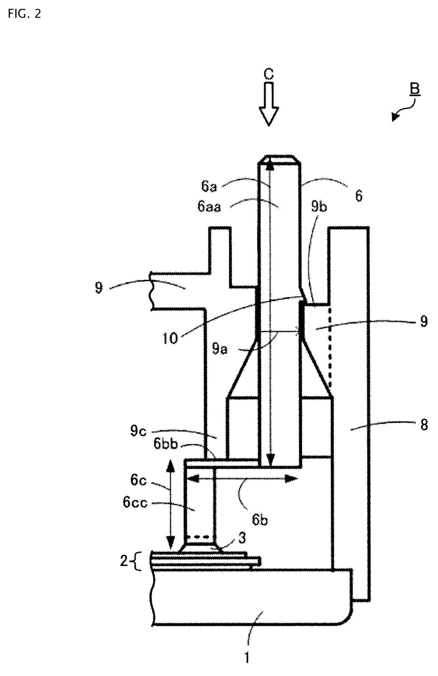
[0055]In addition, FIG. 2 is a cross-sectional diagram illustrating main components of the semiconductor device illustrated in FIG. 1. In addition, FIG. 3 is a diagram for describing main components of the semiconductor device illustrated in FIG. 1. FIG. 2 illustrates enlargement of a vicinity B of a control terminal 6 of the power module 100 illustrated in FIG. 1. FI...

second embodiment

[0081]FIG. 10 is a cross-sectional diagram illustrating main components of a semiconductor device according to a second embodiment of the present invention. In addition, FIG. 11 is a cross-sectional diagram illustrating main components of the semiconductor device illustrated in FIG. 10. FIG. 10 illustrates a cross-sectional diagram of main components at the time of inserting the control terminal 6 constituting a power module 200 into the resin case 7. FIG. 11(a) is a cross-sectional diagram of the control terminal 6 constituting the package 101 of the power module 200 illustrated in FIG. 10 as seen from the side-surface side where the protrusion portion 10 is not installed. FIG. 11(b) is a cross-sectional diagram of the control terminal 6 illustrated in FIG. 11(a) as seen from the side-surface side where the protrusion portion 10 is installed (in the direction indicated by a white leftward arrow K)

[0082]The power module 200 according to the second embodiment is different from the po...

third embodiment

[0085]FIG. 12 is a cross-sectional diagram illustrating main components of a semiconductor device according to a third embodiment of the present invention. FIG. 12 illustrates a cross-sectional diagram of main components at the time of inserting the control terminal 6 constituting a power module 300 into the resin case 7.

[0086]The power module 300 according to the third embodiment is different from the power module according to the first embodiment in that two protrusion portions (hereinafter, referred to as first and second protrusion portions) 10 and 30 are installed in the penetration portion 6a of the control terminal 6 to interpose the cover 9. The first protrusion portion 10 has the same configuration as that of the protrusion portion installed in the penetration portion 6a of the control terminal 6 of the power module according to the first embodiment. The second protrusion portion 30 is installed in the side surface where the first protrusion portion 10 of the control termin...


PUM


Abstract

Aspects of the invention are directed to a power module including a metal base, an insulating substrate which is attached to the metal base, a semiconductor chip and a control terminal which are attached to a circuit pattern of the insulating substrate, and a resin case which is attached to the metal base. The control terminal can include a penetration portion which penetrates a cover of the resin case, an L-shaped processed portion which is connected to the penetration portion, and a connection portion which is connected to the L-shaped processed portion. A protrusion portion can be installed in a portion of the control terminal, which penetrates the cover. The protrusion portion can be in contact with a protrusion receiving portion which is configured with a front surface of the cover. The L-shaped processed portion can be in contact with a convex portion in a rear surface of the cover.

Description

CROSS-REFERENCE TO RELATED APPLICATIONS[0001]This application is a continuation of International Application No. PCT / JP2011 / 068804, filed on Aug. 19, 2011, which is based on and claims priority to Japanese Patent Application No. JP 2010-255762, filed on Nov. 16, 2010. The disclosure of the Japanese priority application and the PCT application in their entirety, including the drawings, claims, and the specification thereof, are incorporated herein by reference.BACKGROUND OF THE INVENTION[0002]1. Field of the Invention[0003]Embodiments of the invention relate to semiconductor devices such as power semiconductor modules (hereinafter, simply referred to as a power modules), where a plurality of semiconductor chips are contained in the same package.[0004]2. Related Art[0005]FIG. 14 is a schematic cross-sectional diagram illustrating a power module in the related art. As illustrated in FIG. 14, a package 501 of a power module 500 is configured to include a metal base 51, an insulating sub...

Claims


Application Information

Patent Timeline
Patent Type & Authority Applications(United States)
IPC IPC(8): H05K1/18H05K1/02
CPCH01L23/043H01L25/18H01L2224/45124H01L2224/32225H01L2224/73265H01L2924/1305H01L23/49811H01L23/3735H01L24/48H01L2224/48227H01L2224/48091H01L2224/48137H01L25/072H01L24/45H05K1/02H05K1/181H01L2924/13055H01L2924/00014H01L2924/00012H01L2924/00H01L24/73H05K1/18
Inventor TAKAMIYA, YOSHIKAZUONISHI, KAZUNAGAKODAIRA, YOSHIHIRO
Owner FUJI ELECTRIC CO LTD
Why Eureka
Try Eureka