System and Method for Detecting Surface Charges of a MEMS Device
- Summary
- Abstract
- Description
- Claims
- Application Information
AI Technical Summary
Benefits of technology
Problems solved by technology
Method used
Image

Examples
Embodiment Construction
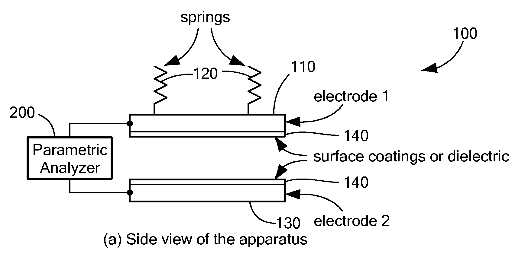
[0005]A first embodiment of the invention involves a method for measuring a retained surface charge within a MEMS device. The MEMS device may include a first and second electrode (e.g., separated by an air gap). The method may first perform an initial signal sweep on the MEMS device by applying a first force signal to the MEMS device and gradually changing the applied first force signal. By changing the first force signal, the method may change a gap between the first and second electrode which, in turn, causes a capacitance change.
[0006]After performing the initial signal sweep, the method may (1) apply a stress signal to the MEMS device for a pre-determined amount of time, and (2) perform at least one additional signal sweep on the MEMS device. The stress signal may cause the first and / or second electrode to retain a surface charge. To perform the additional signal sweep(s), the method may apply a second force signal to the MEMS device and gradually change the applied second force...
PUM
 Abstract
Description
Claims
Application Information
 - R&D
- Intellectual Property
- Life Sciences
- Materials
- Tech Scout
- Unparalleled Data Quality
- Higher Quality Content
- 60% Fewer Hallucinations
Browse by: Latest US Patents, China's latest patents, Technical Efficacy Thesaurus, Application Domain, Technology Topic, Popular Technical Reports.
© 2025 PatSnap. All rights reserved.Legal|Privacy policy|Modern Slavery Act Transparency Statement|Sitemap|About US| Contact US: help@patsnap.com