Electron beam apparatus

a technology of electron beam and apparatus, which is applied in the field of electron beam technique, can solve the problems of inability to maintain the surface charged state, difficulty in making the space between the irradiation position, and disadvantages in measuring and inspection efficiency, and achieves the effect of high throughpu

Active Publication Date: 2011-02-01
HITACHI HIGH-TECH CORP
View PDF8 Cites 49 Cited by
  • Summary
  • Abstract
  • Description
  • Claims
  • Application Information

AI Technical Summary

Benefits of technology

An object of the present invention is to realize an electron beam apparatus which can achieve both of the excellent convergence of the primary beam and the surface charge control. Or, in addition to the above, it has an object to realize an electron beam apparatus which has a higher inspection and measurement throughput than the conventional.
According to the present invention, it is possible to realize an electron beam apparatus which can achieve both of the convergence of the primary beam for signal acquisition and the surface charge control. Further, it is possible to realize an electron beam apparatus which has a high throughput in addition to achieving both of the convergence of the primary beam and the surface charge control by applying the present invention to the electron beam apparatus of multi beam type.

Problems solved by technology

However, the technique described in JP-A-10-294345 has a difficulty in making the space between the irradiation position of the electron beam for inspection and the irradiation position of the electron beam for surface charge control small because of the problem of the size of the electron optical column and the preliminary electron source for irradiation.
For this reason, there is a case where the surface charged state cannot be maintained because the time difference between the electron beam irradiation for surface charge control and the electron beam irradiation for signal acquisition cannot be made to be sufficiently short.
The technique disclosed in JP-A-2002-524827 uses the primary electron beam itself as an electron beam for surface charge control and as it needs to irradiate the same area twice with the same electron beam, it has a disadvantage regarding the measurement and inspection efficiency.

Method used


Image

  • Electron beam apparatus
  • Electron beam apparatus
  • Electron beam apparatus

Examples


embodiment 1

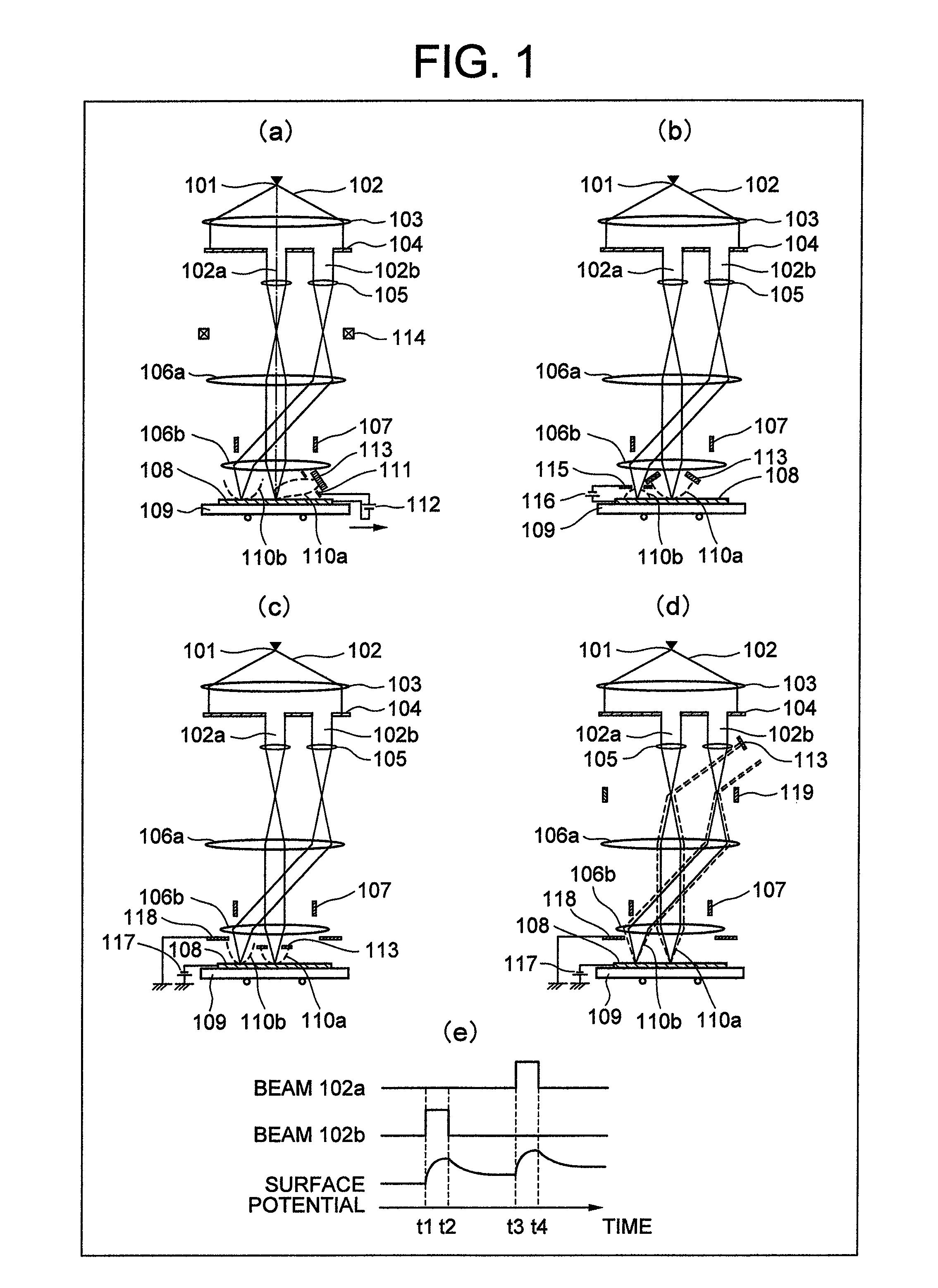
In this embodiment, it will be explained about an embodiment in a so-called scanning electron microscope of single beam type. First, the type of the electron beam apparatus of this embodiment will be explained using FIGS. 1(a) to 1(d).

FIG. 1(a) is a diagram showing a schematic configuration of an electron optical system of the electron microscope according to the first embodiment. The electron optical system shown in FIG. 1(a) is configured with an electron source 101, a condenser lens configured with electromagnetic lens 103, an aperture array having a plurality of holes 104, a illumination optical system configured with a lens array 105, an object lenses 106a, 106b, a deflector to deflect a beam to scan a sample 107, etc., a detection optical system configured with a secondary electron detector 113, a collector electrode 111 to collect a secondary charged particle 110a generated by the irradiation of a primary beam 102a, etc., a stage 109, etc. Though not shown, the above-mentione...

embodiment 2

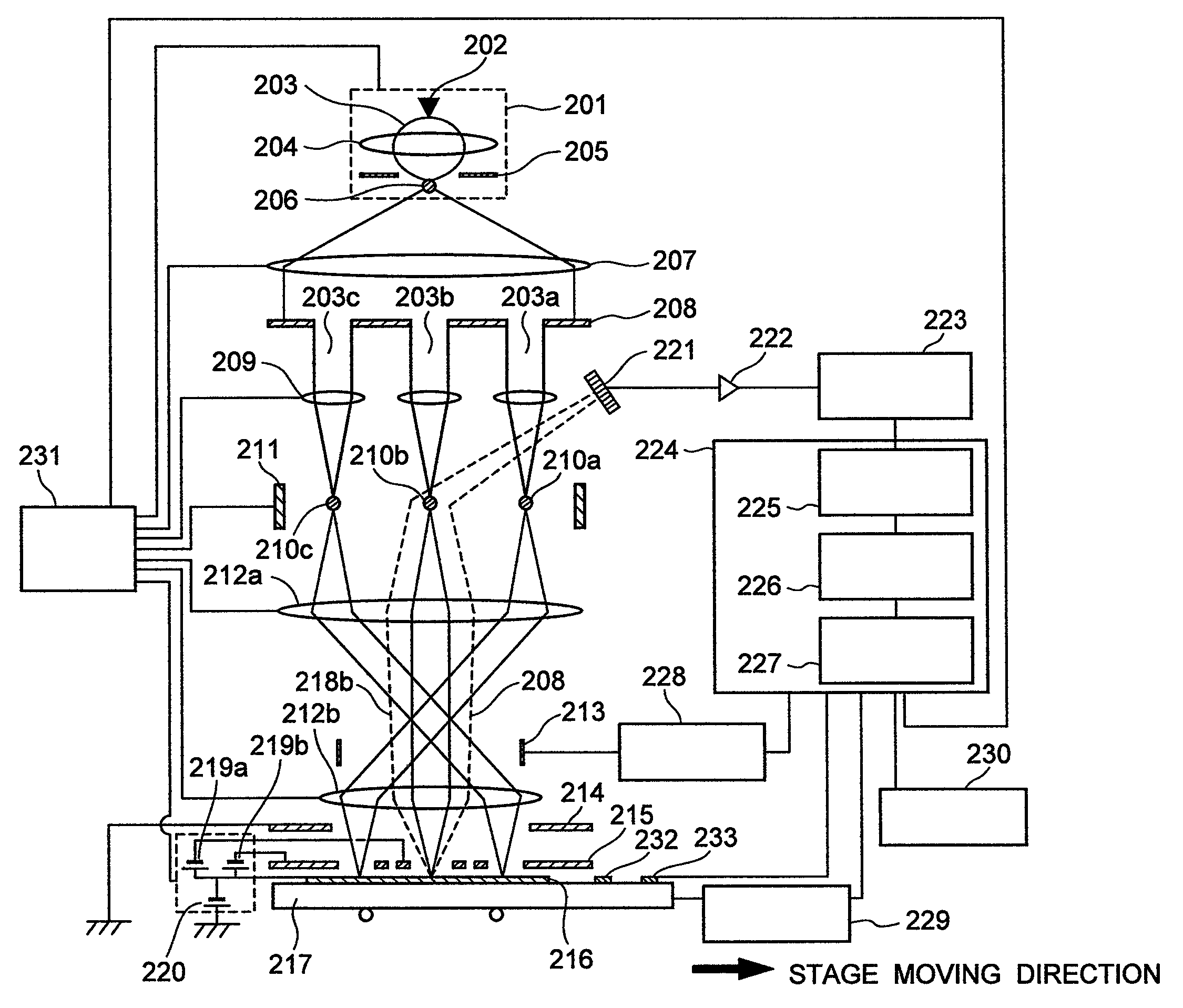
In this embodiment, it will be explained about an apparatus configuration in the scanning electron microscope of multi beam type which separates the electron beam emitted from the same electron source into a plurality of electron beams and uses at least one or more than one electron beams as an electron beam for surface charge control.

FIG. 2 is a diagram showing a schematic configuration of an electron beam inspection apparatus according to a second embodiment of the present invention. In this embodiment, it is configured being provided with an electric field strength control unit which makes the potential distributions on the sample different distributions in the irradiation positions of the primary beam for surface charge control and the primary beam for inspection. More specifically, a surface electric field control electrode is installed as this electric field strength control unit to control the electric field distribution on the sample. It will be described in detail later abo...

embodiment 3

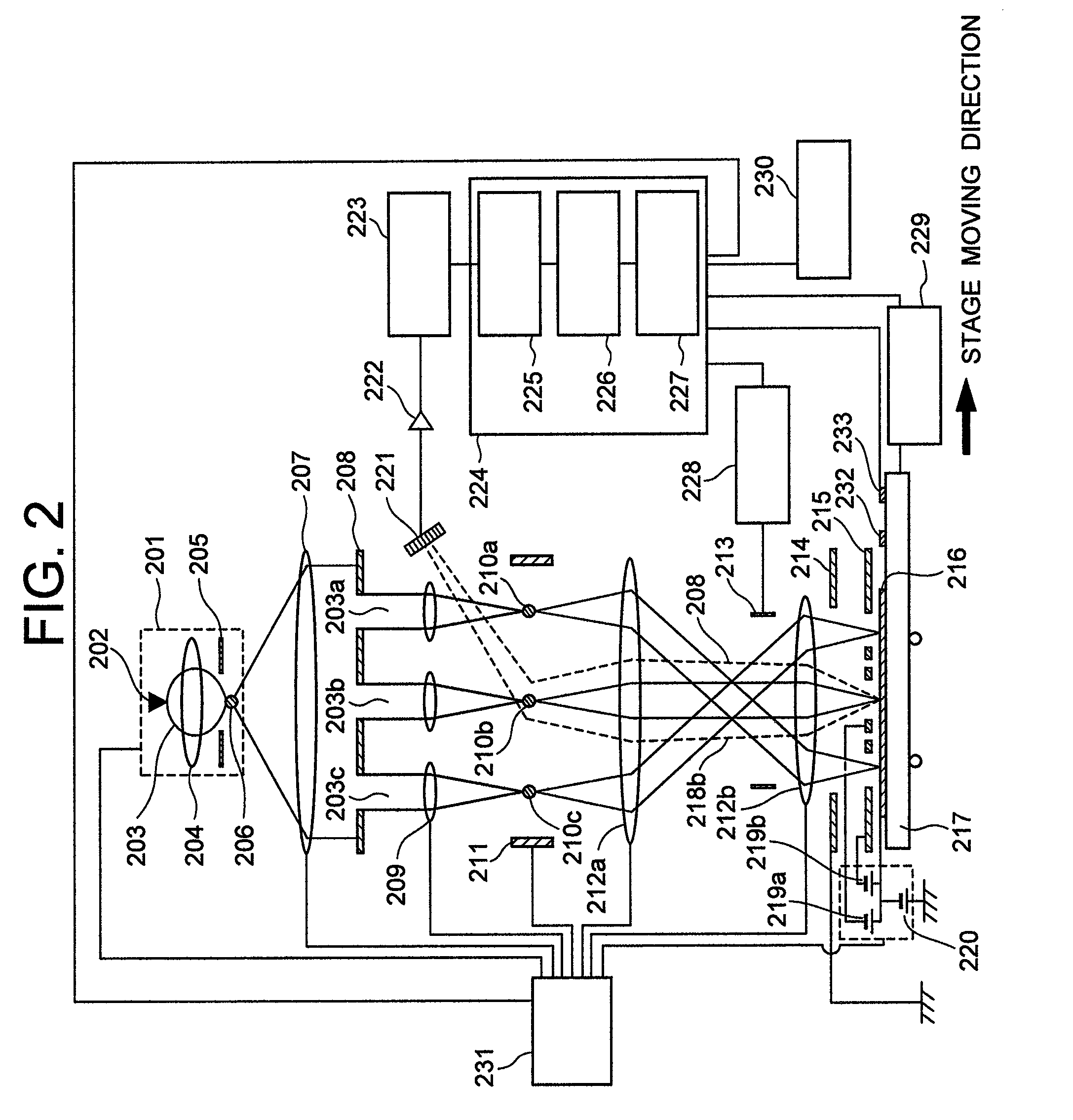
In the embodiment 2 the primary beam is split into three beams using the aperture array and the two of them are used for surface charge control and the one is for inspection. On this occasion, the almost equal current is given to the three primary beams by making the diameters of the plurality of apertures of the aperture array equal. However, with this embodiment there is a case where the irradiation intensity of the primary beam for surface charge control is not sufficient and the wafer is not surface charged sufficiently.

Then, in this embodiment, it is attempted to enlarge the current of the primary beam for surface charge control. FIG. 7 is a diagram showing a schematic configuration of an electron beam inspection apparatus according to a third embodiment of the present invention. In this embodiment also, in the same way as the embodiment 2, the primary beam is split into three primary beams 203a, 203b, 203c using the aperture array and among these 203a and 203c are used as the ...


PUM


Abstract

A plurality of primary beams are formed from a single electron source, the surface charge of a sample is controlled by at least one primary beam, and at the same time, the inspection of the sample is conducted using a primary beam other than this. Also, for an exposure area of the primary beam for surface charge control and an exposure area of the primary beam for the inspection, the surface electric field strength is set individually. Also, the current of the primary beam for surface charge control and the interval between the primary beam for surface charge control and the primary beam for inspection are controlled.

Description

CLAIM OF PRIORITYThe present application claims priority from Japanese application JP 2006-350839 filed on Dec. 27, 2006, the content of which is hereby incorporated by reference into this application.BACKGROUND OF THE INVENTIONThe present invention relates to the electron beam technique, and in particular, to an electron beam apparatus such as an inspection apparatus, a microscope, etc. used in the semiconductor process, etc.In the semiconductor process, a variety of kinds of electron beam apparatus are used with the aim of the observation of the circuit pattern formed on the wafer and the chip, the measurement, the defect review and classification, the inspection, etc. In these electron beam apparatus, the above-mentioned observation, measurement, defect review and classification, inspection, etc. are conducted by irradiating an electron beam called a primary beam on a sample and performing a variety of kinds of operation process for a signal obtained by detecting a secondary elec...

Claims


Application Information

Patent Timeline
Patent Type & Authority Patents(United States)
IPC IPC(8): H01J37/26
CPCH01J37/244H01J37/28H01J2237/0435H01J2237/2448H01J2237/24564H01J2237/24592
Inventor TANIMOTO, SAYAKAOHTA, HIROYAMAKINO, HIROSHIFUNATSU, RYUICHI
Owner HITACHI HIGH-TECH CORP
Why Eureka
Try Eureka