

Stress reduction means for warp control of substrates through clamping
a clamping and stress reduction technology, applied in the direction of soldering equipment, manufacturing tools, auxillary welding devices, etc., can solve the problems of large sample to sample variation (sigma) of warp, thermal warp, and potential non-wet or unequal c4 solder height, so as to minimize the variation in the height of the solder ball
- Summary
- Abstract
- Description
- Claims
- Application Information
AI Technical Summary
Benefits of technology
Problems solved by technology
Method used
Image

Examples
first embodiment
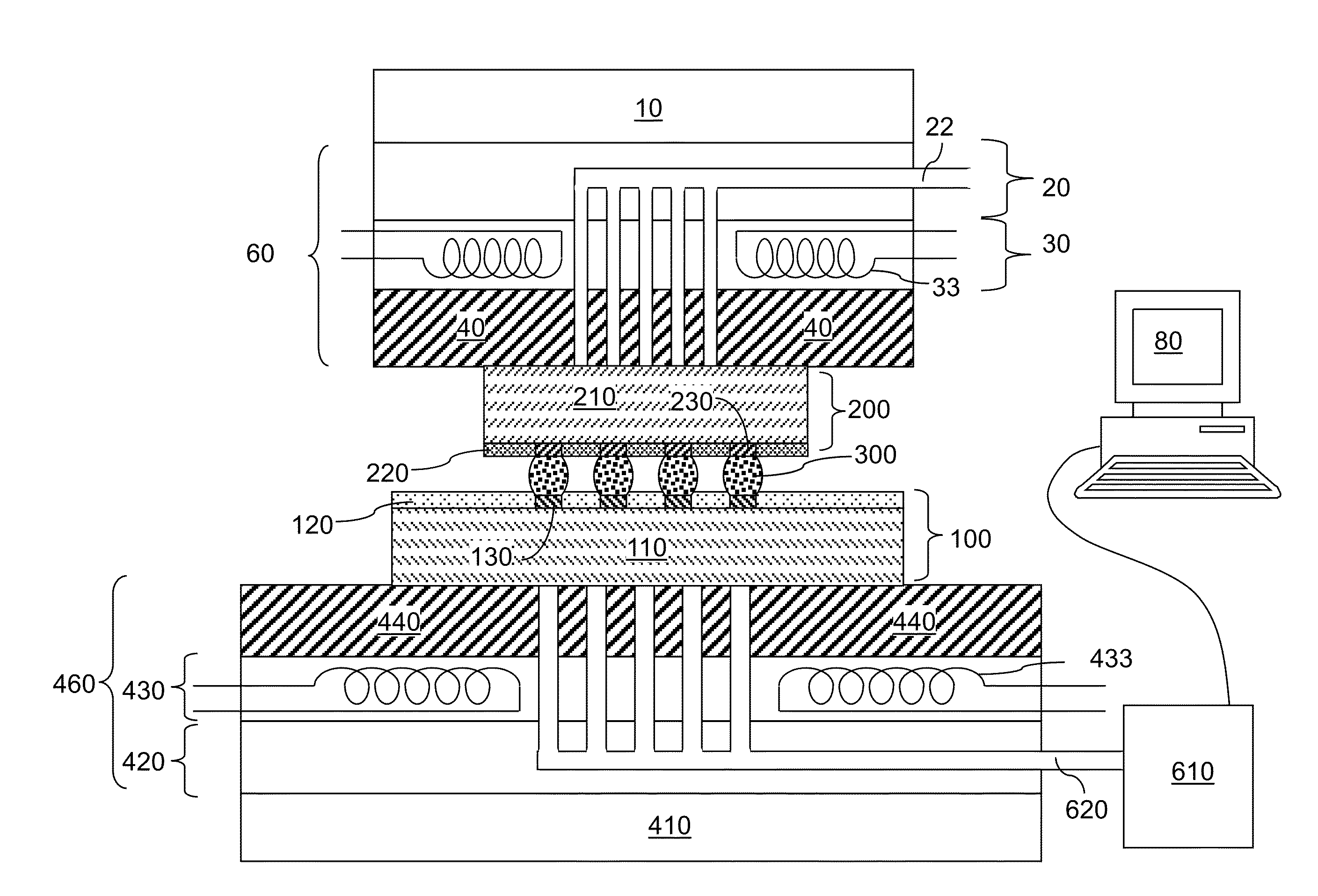
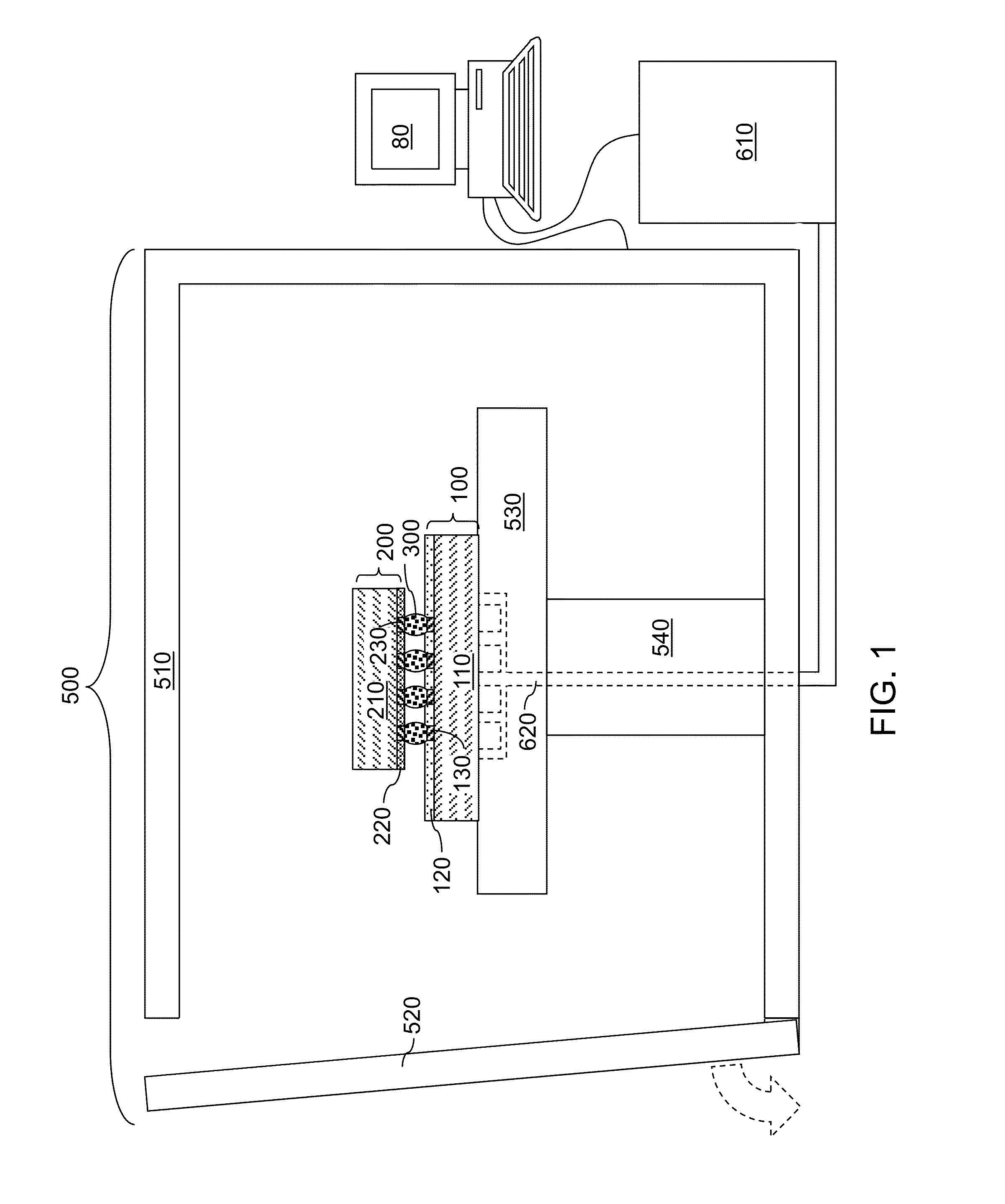
[0025]Referring to FIG. 1, a first exemplary apparatus according to the present disclosure is illustrated, which can be employed for bonding a first substrate 100 to a second substrate 200.
[0026]The first substrate 100 can include a first substrate layer 110, a first surface dielectric layer 120, and an array of first bonding pads 130 embedded within the first surface dielectric layer 120. The first substrate 100 can be a packaging substrate or a semiconductor chip or an interposer. If the first substrate 100 is a packaging substrate, the first substrate 100 can include layers of wiring structures (metal interconnect structures), and can be a ceramic substrate, an organic laminated substrate, a silicone substrate, a metal substrate, or a flexible film substrate. If the first substrate 100 is a semiconductor chip, the first substrate 100 includes semiconductor devices therein.
[0027]The second substrate 200 includes a second substrate layer 210, a second surface dielectric layer 220, ...
second embodiment
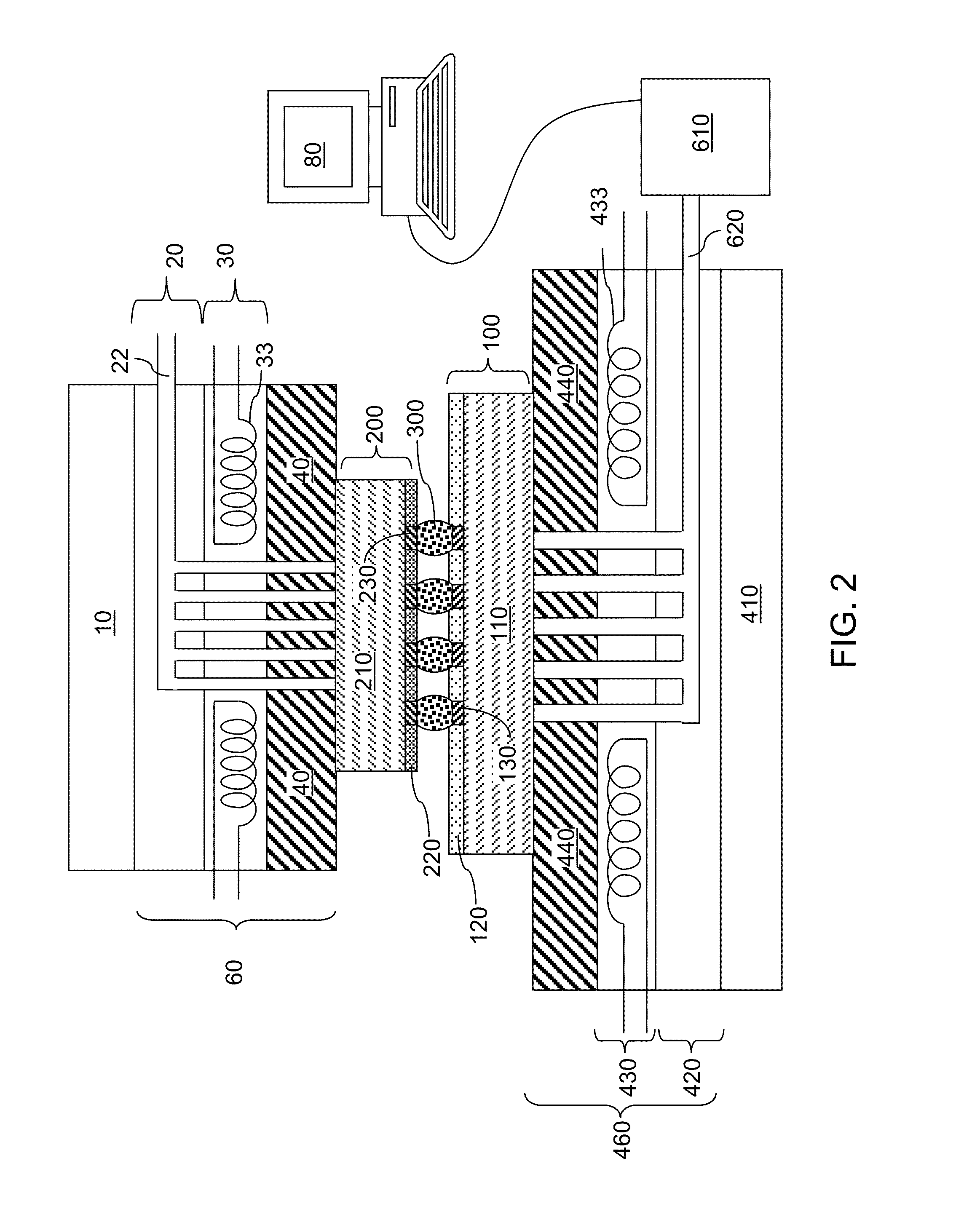
[0040]Referring to FIG. 2, a second exemplary apparatus according to the present disclosure includes a chip bonder configured to hold, and bond, a first substrate 100 and a second substrate 200. The second exemplary structure includes a bonder head 60, the first substrate 100, an array of solder material portions 300, the second substrate 200, and a base plate 460 that functions as a platform to support the first substrate 100. A back side of the second substrate 200 can be attached to the bottom side of the bonder head 60 by vacuum suction. A bonder head movement actuator 10 configured to provide vertical movement of the bonder head 60 relative to the base plate 460 can be located above the bonder head 60. The first substrate 100 can be any of a semiconductor chip, an interposer, or a packaging substrate. The second substrate 200 can be any of a semiconductor chip, an interposer, or a packaging substrate.
[0041]The bonder head movement actuator 10 can operate to enable the vertical ...
PUM
| Property | Measurement | Unit |
|---|---|---|
| melting temperature | aaaaa | aaaaa |
| temperature | aaaaa | aaaaa |
| temperature | aaaaa | aaaaa |
Abstract
Description
Claims
Application Information