

Non-bridging contact via structures in proximity
a contact via and proximity technology, applied in the direction of semiconductor devices, semiconductor/solid-state device details, electrical devices, etc., can solve the problems of limiting the scaling of dimensions of the via hole, the proximity of the adjacent pair of contact via holes is prone to bridging, and the lithographic resolution of the contact hole is limited
- Summary
- Abstract
- Description
- Claims
- Application Information
AI Technical Summary
Benefits of technology
Problems solved by technology
Method used
Image

Examples
Embodiment Construction
[0054]As stated above, the present disclosure relates to methods for forming trenches having different widths and the same depth, which are now described in detail with accompanying figures. Throughout the drawings, the same reference numerals or letters are used to designate like or equivalent elements. The drawings are not necessarily drawn to scale.
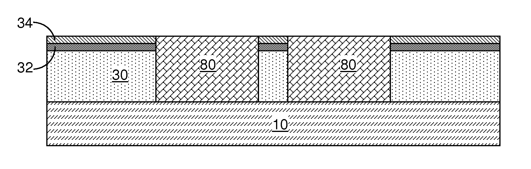
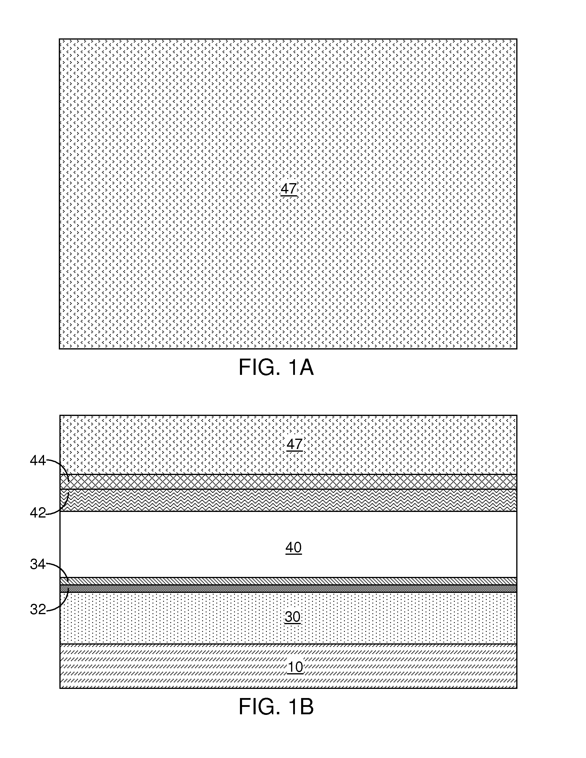
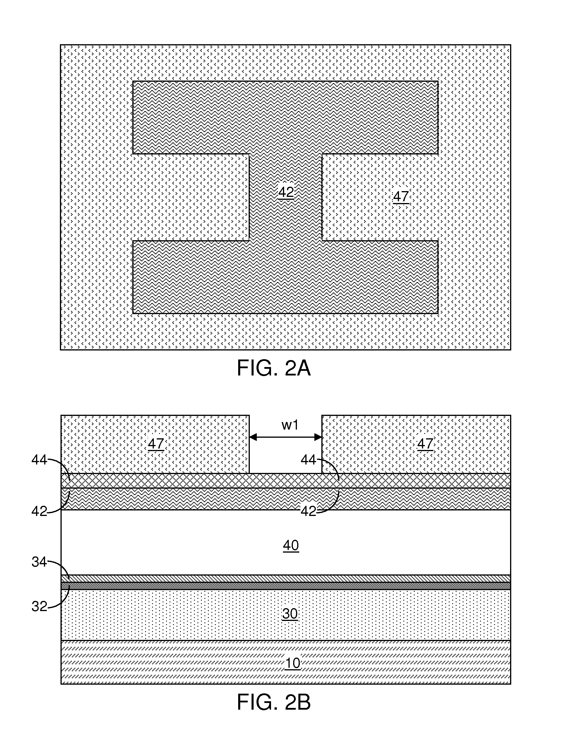
[0055]Referring to FIGS. 1A and 1B, a first exemplary structure according to a first embodiment of the present disclosure includes a stack of a substrate layer 10, at least one underlying material layer, a template layer 40, and at least one photosensitive-material-including layer. The at least one underlying material layer can include, for example, a dielectric material layer 30, an optional cap material layer 32, and an optional hard mask layer 34. The at least one photosensitive-material-including layer can include, for example, a stack of a first organic planarization layer 42, a first antireflective coating (ARC) layer 44, and a f...
PUM
 Abstract
Description
Claims
Application Information