Multi-exposure lithography employing a single Anti-reflective coating layer

a technology of anti-reflective coating and multi-exposure lithography, which is applied in the direction of photomechanical treatment originals, instruments, photomechanical equipment, etc., can solve the problems of difficult to obtain light sources that provide reduced wavelengths in the deep ultraviolet (duv) or extreme ultraviolet (euv) range, and the inability to obtain adequate light sources to enable printing of dimensions less than 50 nm,

Inactive Publication Date: 2010-01-14
IBM CORP +1
View PDF10 Cites 15 Cited by
  • Summary
  • Abstract
  • Description
  • Claims
  • Application Information

AI Technical Summary

Problems solved by technology

While developments are under way to provide high numerical aperture exposure systems and/or increase the coefficient k to minimum feature size F, the rate of reduction of the minimum feature size F through such efforts is far slower than the rate of reduction of desired feature sizes for high performance of semiconductor devices.
Further, obtaining light sources that provide reduced wavele...

Method used


Image

  • Multi-exposure lithography employing a single Anti-reflective coating layer
  • Multi-exposure lithography employing a single Anti-reflective coating layer
  • Multi-exposure lithography employing a single Anti-reflective coating layer

Examples


Embodiment Construction

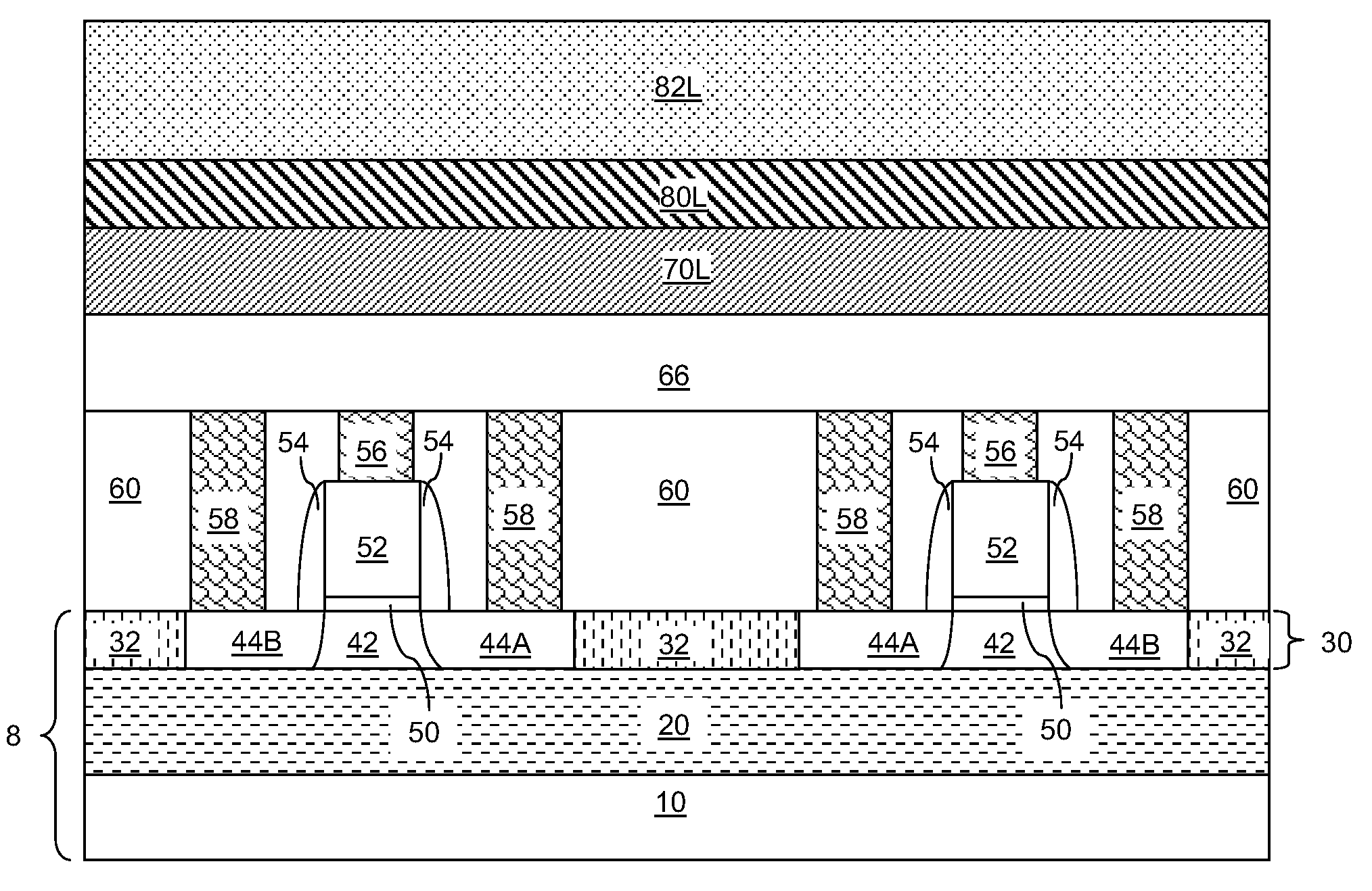
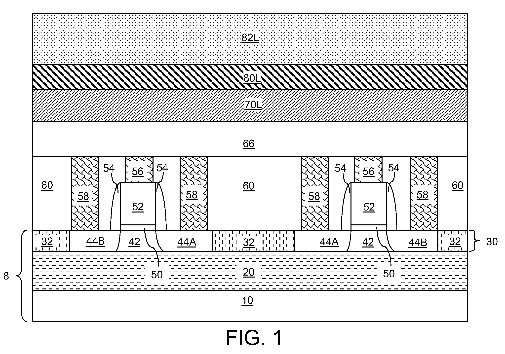
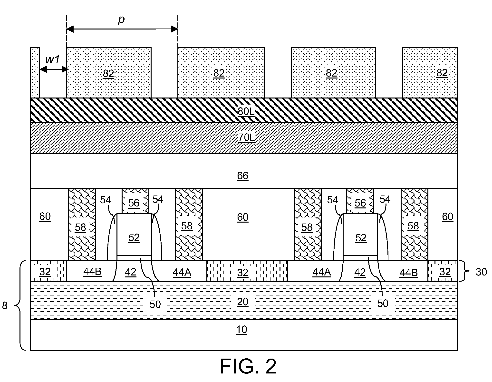
[0032]As stated above, the present invention relates to methods for multi-exposure lithography employing a single anti-reflective coating (ARC) layer and structures for effecting the same, which are now described in detail with accompanying figures. As used herein, when introducing elements of the present invention or the preferred embodiments thereof, the articles “a”, “an”, “the” and “said” are intended to mean that there are one or more of the elements. Throughout the drawings, the same reference numerals or letters are used to designate like or equivalent elements. Detailed descriptions of known functions and constructions unnecessarily obscuring the subject matter of the present invention have been omitted for clarity. The drawings are not necessarily drawn to scale.

[0033]Referring to FIG. 1, a first exemplary lithographic structure according to a first embodiment of the present invention comprises a semiconductor structure including a semiconductor substrate 8, semiconductor d...


PUM

PropertyMeasurementUnit
Structureaaaaaaaaaa
Sizeaaaaaaaaaa
Adhesion strengthaaaaaaaaaa

Abstract

A first photoresist is applied over an optically dense layer and lithographically patterned to form an array of first photoresist portions having a pitch near twice a minimum feature size. The pattern in the first photoresist portions, or a first pattern, is transferred into the ARC layer and partly into the optically dense layer. A second photoresist is applied and patterned into another array having a pitch near twice the minimum feature size and interlaced with the first pattern. The pattern in the second photoresist, or a second pattern, is transferred through the ARC portions and partly into the optically dense layer. The ARC portions are patterned with a composite pattern including the first pattern and the second pattern. The composite pattern is transferred through the optically dense layer and into the underlayer to form a sublithographic pattern in the underlayer.

Description

FIELD OF THE INVENTION[0001]The present invention relates to semiconductor processing methods, and particularly to methods for multi-exposure lithography employing a single anti-reflective coating (ARC) layer, and structures for effecting the same.BACKGROUND OF THE INVENTION[0002]Lithography is employed in semiconductor manufacturing to pattern features in a photoresist. A layer of photoresist is exposed to incident light, which may be deep-ultraviolet (DUV) radiation, mid-ultraviolet (MUV) radiation, or X-ray radiation. Alternately, the layer of photoresist may be exposed to energetic electron in e-beam lithography. The energy of the photons or electrons causes changes in chemical composition of exposed portions of the photoresist, for example, by cross-linkage, scission, side chain removal, etc. Pre-baking or post-baking of the photoresist may be employed to maximize the changes in the chemical properties of the exposed portion of the photoresist relative to unexposed portions of ...

Claims


Application Information

Patent Timeline
IPC IPC(8): G03F7/20B32B9/00
CPCG03F7/70466G03F7/70958Y10T428/24802H01L21/76838G03F7/20H01L21/76816
Inventor BASKER, VEERARAGHAVAN S.CONLEY, WILLARD E.HOLMES, STEVEN J.HORAK, DAVID V.
Owner IBM CORP
Why Eureka
Try Eureka