High density plasma CVD process for making dielectric anti-reflective coatings

a plasma cvd and anti-reflective technology, applied in the field of high density plasma cvd process for making dielectric anti-reflective coatings, can solve the problems of resist contamination, .2 gas cannot be used, and the resist profile is abnormal

Inactive Publication Date: 2000-05-09
POLARIS INNOVATIONS LTD
View PDF15 Cites 84 Cited by
  • Summary
  • Abstract
  • Description
  • Claims
  • Application Information

AI Technical Summary

Problems solved by technology

Any environmental contamination, or other acid depleting process or substrate contamination effects can cause abnormal resist profiles.
In this pressure range, O.sub.2 gas cannot be used because of explosion risk.
Accordingly, one significant disadvantage of prior methods of preparing silicon oxynitride DARC is the presence of resist contamination, and this resist contamination remains intact despite the use of additional silicon dioxide and / or plasma treatment to oxidize the surface of silicon oxynitride.
Another disadvantage of the prior art processes of preparing silicon oxynitride DARC is that, when a RF PECVD is utilized, the process must proceed in a vacuum system at a pressure range of from about 1 torr to about 20 torr, most typically, deposition of the DARC films are deposited at a pressure range of from about 1.5 torr 10 torr; however, in this pressure range, O.sub.2 gas cannot be used due to the risk of explosion.
A further disadvantage of prior methods of preparing silicon oxynitride DARC is that, since O.sub.2 gas cannot be used due to explosion risk, N.sub.2 O gas is used as an oxygen source for both silicon oxynitride and silicon dioxide; however, the use of the N.sub.2 O gas when an additional silicon dioxide film is used as a barrier layer renders the process at risk of containing nitrogen and / or an amine group from the N.sub.2 O reaction gas.
Therefore, depending upon the sensitivity of the chemically amplified photoresist to the nitrogen content in the substrate film, extremely small amounts of the amine group or dangling bonds at the surface tend to cause photoresist contamination, as evidenced by a "foot" over a nitrogen containing substrate, such as silicon oxynitride, silicon nitride, and titanium nitride.

Method used


Image

  • High density plasma CVD process for making dielectric anti-reflective coatings
  • High density plasma CVD process for making dielectric anti-reflective coatings
  • High density plasma CVD process for making dielectric anti-reflective coatings

Examples


Embodiment Construction

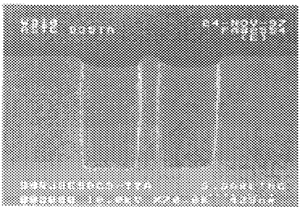
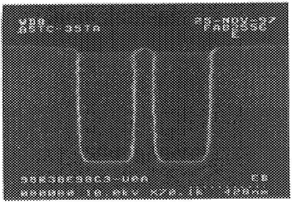
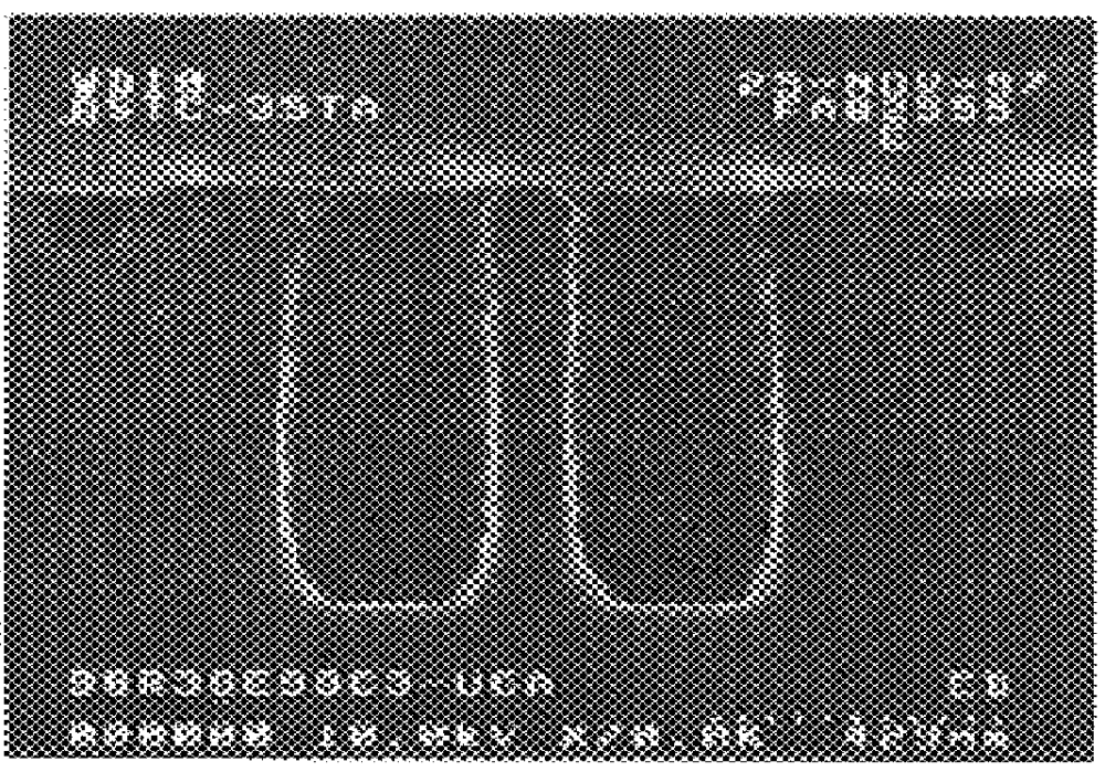
In a vacuum reactor chamber, silicon oxynitride DARC and silicon dioxide are deposited using a high density plasma (HDP) CVD process, and any frequency and any combination of RF powers is used for source power at a range of between 50 watts and about 5,000 watts and at low pressure ranges in the vacuum chamber of between about 0.1 mtorr and about 20 mtorr. The bias power for Ar sputtering is between the range of 0 watts and about 4,000 watts, and O.sub.2 gas is used as an oxygen source of DARC. The O.sub.2 gas flow rate during deposition is between about 1 sccm and about 500 sccm, and the N.sub.2 flow rate during deposition is between about 0 sccm and about 500 sccm.

In one embodiment of the invention, when silicon oxynitride is deposited, use is made of SiH.sub.4 / O.sub.2 / N.sub.2 chemistry, and the high density plasma (HDP) silicon oxynitride film obtained is denser and cleaner film then conventional film. This is very positive, since the HDP silicon oxynitride can be used without ...


PUM

PropertyMeasurementUnit
pressureaaaaaaaaaa
pressureaaaaaaaaaa
vacuumaaaaaaaaaa

Abstract

An improved process for preparing nitrogen containing substrates selected from the group consisting of silicon oxynitride, silicon nitride and titanium nitride films and silicon dioxide cap films characterized by prevent resist contamination when used as dielectric anti-reflective coatings, using a high density plasma CVD system, comprising: providing a processing chamber holding a wafer in a vacuum sufficient to enable O2 to be used as an oxygen source without risk of explosion in a plasma generating region of the processing chamber; introducing a gaseous mixture selected from the group consisting of SiH4 / O2 / N2 or SiH4 / O2 / N2 / Ar into the processing chamber; and subjecting the processing chamber to a RF electrical signal of sufficient frequency to create a high density plasma in the plasma generating region of said processing chamber, whereby said wafer is processed by resulting high density plasma generated by said RF electrical signal.

Description

1. Field of the InventionThe invention is directed to a process of depositing silicon oxynitride and silicon dioxide in a manner such that these chemically amplified photoresist are not contaminated from amine groups or dangling bonds as a result of using high density plasma(HDP). In general, the invention is accomplished by depositing silicon oxynitride DARC and silicon dioxide using a high density plasma (HDP) CVD system at a lower than usual pressure range and at higher power, thereby permitting the use of O.sub.2 gas as an oxygen source of DARC.2. Description of the Prior ArtSilicon oxynitride DARC, has been broadly used for DUV lithography, and is especially attractive for improving lithographic process windows because of its tunable refractive index and high etch selectivity to resist. Resist contamination is one of the greater concerns in the use or application of silicon oxynitride films; especially due to the presence of amine radicals, which are known to contaminate chemic...

Claims


Application Information

Patent Timeline
Patent Type & Authority Patents(United States)
IPC IPC(8): C23C16/40C23C16/34C23C16/30H01L21/027H01L21/02H01L21/31C23C16/42H01L21/205
CPCC23C16/308C23C16/34H01L21/0276C23C16/402C23C16/345C23C16/505
Inventor LEE, GILL YONG
Owner POLARIS INNOVATIONS LTD
Why Eureka
Try Eureka