Thin two sided single crystal solar cell and manufacturing process thereof

a solar cell, two-sided technology, applied in the field of solar cell manufacturing, can solve the problems of loss of light-generated electrons near the surface of the solar cell, limited thermal diffusion characteristics of the bulk material dopant profile created by the furnace diffusion, etc., and achieves the effects of high material quality, high thermal reorganization of silicon, and high material quality

Inactive Publication Date: 2010-05-06
CRYSTAL SOLAR INC
View PDF10 Cites 84 Cited by
  • Summary
  • Abstract
  • Description
  • Claims
  • Application Information

AI Technical Summary

Benefits of technology

[0014]According to one aspect of the present invention, fabrication starts with a conventional thick monocrystalline silicon wafer on one surface of which a porous layer has been created, typically by an electrochemical etching process. After creation of the porous layer, which typically has a thickness of 2 to 5 microns, the wafer may be heated to induce sufficient thermal reorganization of the silicon on the upper surface of the porous layer to enable high quality epitaxial growth of subsequent films to occur.
[0015]The growth of films using epitaxial deposition affords high materials quality as compared with the conventional method of manufacturing silicon wafers. In addition, with the formation of P-N junctions during epitaxial deposition, the possibility exists for much better control of dopant profiles including sharp junction interfaces compared with dopant profiles generated using conventional furnace diffusion. This control arises because the epitaxial growth process allows the control of dopant concentrations in the material as it is deposited and this control is accomplished by the regulation and variation of the various feed gases during the epitaxial deposition process. Dopant profiles created in the bulk material by means of furnace diffusion, in contrast, are limited by the characteristics of thermal diffusion. In addition, at the surface, the formation of precipitates of the dopant species (e.g. phosphorus) may also occur, creating an undesirable layer which can cause loss of light-generated electrons near the surface of the solar cell. Thus, the use of epitaxial deposition for the growth of the necessary P- and N-type regions in the PV cell structure of the present invention affords many advantages over prior art PV cells structures fabricated using furnace diffusion.

Problems solved by technology

Dopant profiles created in the bulk material by means of furnace diffusion, in contrast, are limited by the characteristics of thermal diffusion.
In addition, at the surface, the formation of precipitates of the dopant species (e.g. phosphorus) may also occur, creating an undesirable layer which can cause loss of light-generated electrons near the surface of the solar cell.

Method used


Image

  • Thin two sided single crystal solar cell and manufacturing process thereof
  • Thin two sided single crystal solar cell and manufacturing process thereof
  • Thin two sided single crystal solar cell and manufacturing process thereof

Examples


Embodiment Construction

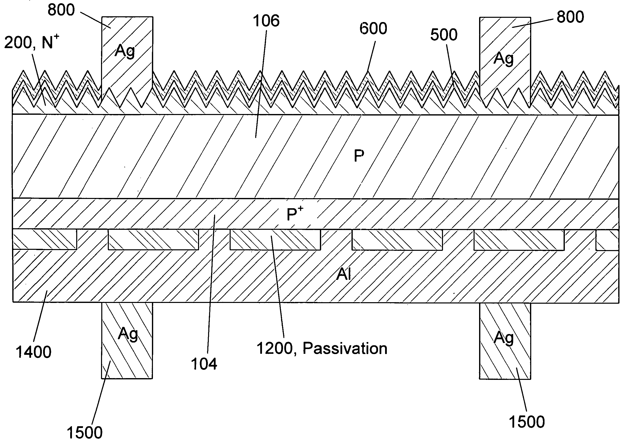
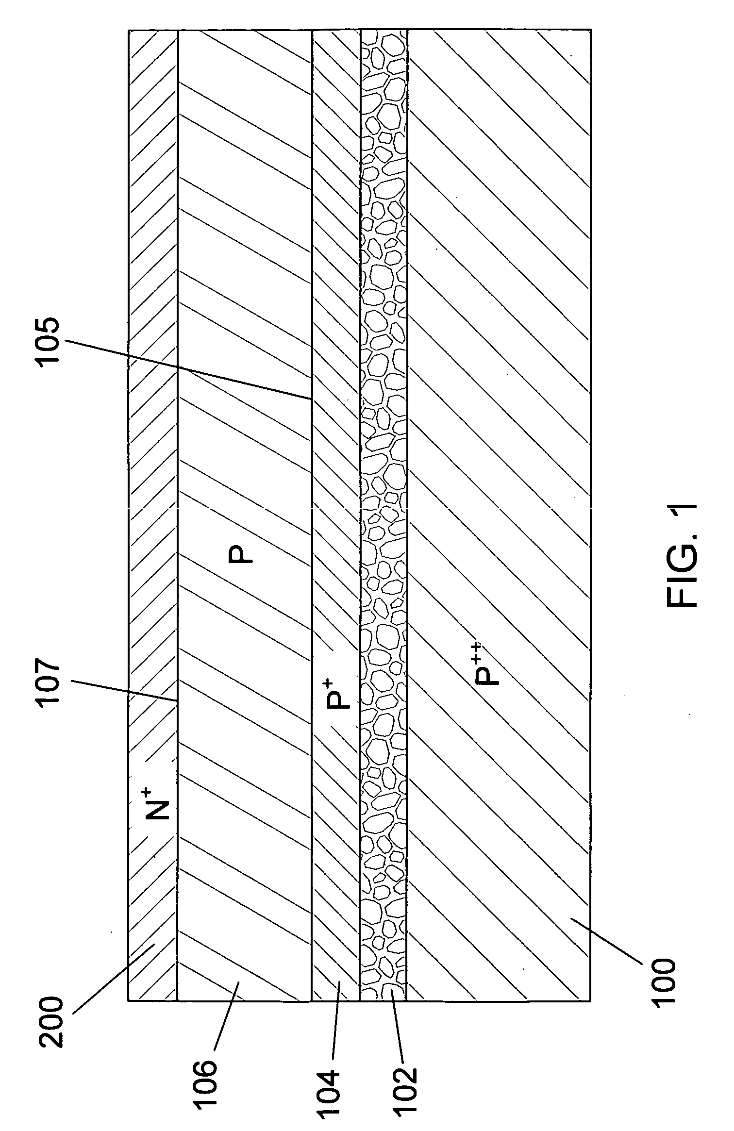
[0041]FIGS. 1 to 13 illustrate exemplary steps in the fabrication process for a thin photovoltaic cell according to one embodiment of the invention. Most figures are schematic side cross-sectional views in which the vertical dimensions are greatly enlarged relative to the horizontal dimensions. Note that this exaggeration of the vertical scale makes the profiles of the isotropic etch steps appear as vertical lines since any undercutting occurring during the isotropic etch process cannot be seen when the vertical scale is greatly enlarged.

[0042]A silicon photovoltaic (PV) wafer 100 illustrated in the schematic side cross-section view of FIG. 1 is a single-crystal wafer of the type used for semiconductor integrated circuits or can be of solar grade which has typically been used in conventional single crystal silicon solar cells. Four layers are grown on its top surface: a thin porous silicon layer 102, a P+-type layer 104, a P-type layer 106, and an N+-type layer 200. In this embodime...


PUM

PropertyMeasurementUnit
thicknessaaaaaaaaaa
thicknessaaaaaaaaaa
thicknessaaaaaaaaaa

Abstract

A design and manufacturing method for a photovoltaic (PV) solar cell less than 100 μm thick are disclosed. A porous silicon layer is formed on a wafer substrate. Portions of the PV cell are then formed using diffusion, epitaxy and autodoping from the substrate. All front side processing of the solar cell (junctions, passivation layer, anti-reflective coating, contacts to the N+-type layer) is performed while the thin epitaxial layer is attached to the porous layer and substrate. The wafer is then clamped and exfoliated. The back side of the PV cell is completed from the region of the wafer near the exfoliation fracture layer, with subsequent removal of the porous layer, passivation, patterning of contacts, deposition of a conductive coating, and contacts to the P+-type layer. During manufacturing, the cell is always supported by either the bulk wafer or a wafer chuck, with no processing of bare thin PV cell

Description

CROSS-REFERENCE TO RELATED APPLICATIONS[0001]This application claims the benefit of U.S. Provisional Application Ser. No. 61 / 068,629, filed Mar. 8, 2008, which is expressly incorporated by reference herein.BACKGROUND OF THE INVENTION[0002]1. Field of the Invention[0003]This invention relates generally to the field of solar cell manufacturing, and more particularly to methods of manufacturing solar cells formed using thin epitaxial films grown on single crystal silicon wafer substrates.[0004]2. Description of the Related Art[0005]The majority of single crystal silicon photovoltaic (PV) solar cells fabricated today employ contacts on both the front and back surfaces, with doping of the diode structure in the PV cell done using conventional furnace diffusion of boron (P-type) or phosphorous (N-type) dopants. Typically, prior art fabrication processes for photovoltaic (PV) solar cells use thick wafers (typical thickness of about 180 μm) for the substrate. A sequence of furnace diffusion...

Claims


Application Information

Patent Timeline
Patent Type & Authority Applications(United States)
IPC IPC(8): H01L31/00H01L21/306H01L31/18
CPCH01L31/022425H01L31/072H01L31/1804H01L31/1892Y02E10/547Y02P70/521Y02P70/50
Inventor RAVI, KRAMADHATI V.
Owner CRYSTAL SOLAR INC
Why Eureka
Try Eureka