Quantum dot optoelectronic device having an sb-containing overgrown layer

Inactive Publication Date: 2008-10-23
NAT CENT UNIV
View PDF9 Cites 10 Cited by
  • Summary
  • Abstract
  • Description
  • Claims
  • Application Information

AI Technical Summary

Benefits of technology

[0004]The present invention proposes a quantum dot optoelectronic device having an Sb-containing overgrown layer to im

Problems solved by technology

Yet, by doing so, the confinement potential of the carriers in quantum dot structure is lowered by the InGaAs; or, the light emission efficiency is reduced due to the poor crystal quality of InAlAs grown at low temperature.
Besides, growing a heterostructure containing indium

Method used


Image

  • Quantum dot optoelectronic device having an sb-containing overgrown layer
  • Quantum dot optoelectronic device having an sb-containing overgrown layer
  • Quantum dot optoelectronic device having an sb-containing overgrown layer

Examples


Example

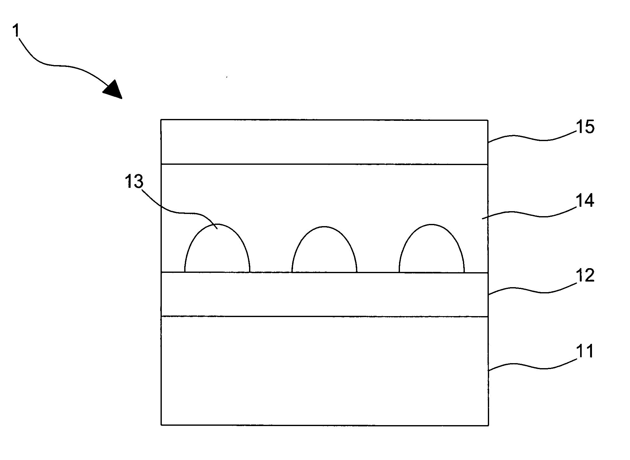
[0024]Shown in FIG. 3A is a schematic structure showing the first embodiment of this invention. As shown in the figure, a quantum dot optoelectronic device 1a comprises an epitaxy substrate 11a, an epitaxy buffer layer 12a, a quantum dot layer 13a, an overgrown layer 14a and a surface layer 15a, where the epitaxy substrate 11a, the epitaxy buffer layer 12a, and the surface layer 15a are made of GaAs; the quantum dot structure 13a is made of InAs; and the overgrown layer 14a is made of InGaAsSb.

[0025]FIG. 3B is an energy band diagram of the first embodiment of this invention, showing the band gaps of the quantum dot 21, the overgrown layer 22 and GaAs 23. The confinement potential for the carriers is increased by the InGaAsSb overgrown layer compared to the prior arts because both the band gap of the InGaAsSb overgrown layer moves upward with respective to the band gap of InAs quantum dot. Therefore, thermal e escape of electrons and holes out of the quantum dot is reduced.

[0026]FIG....

Example

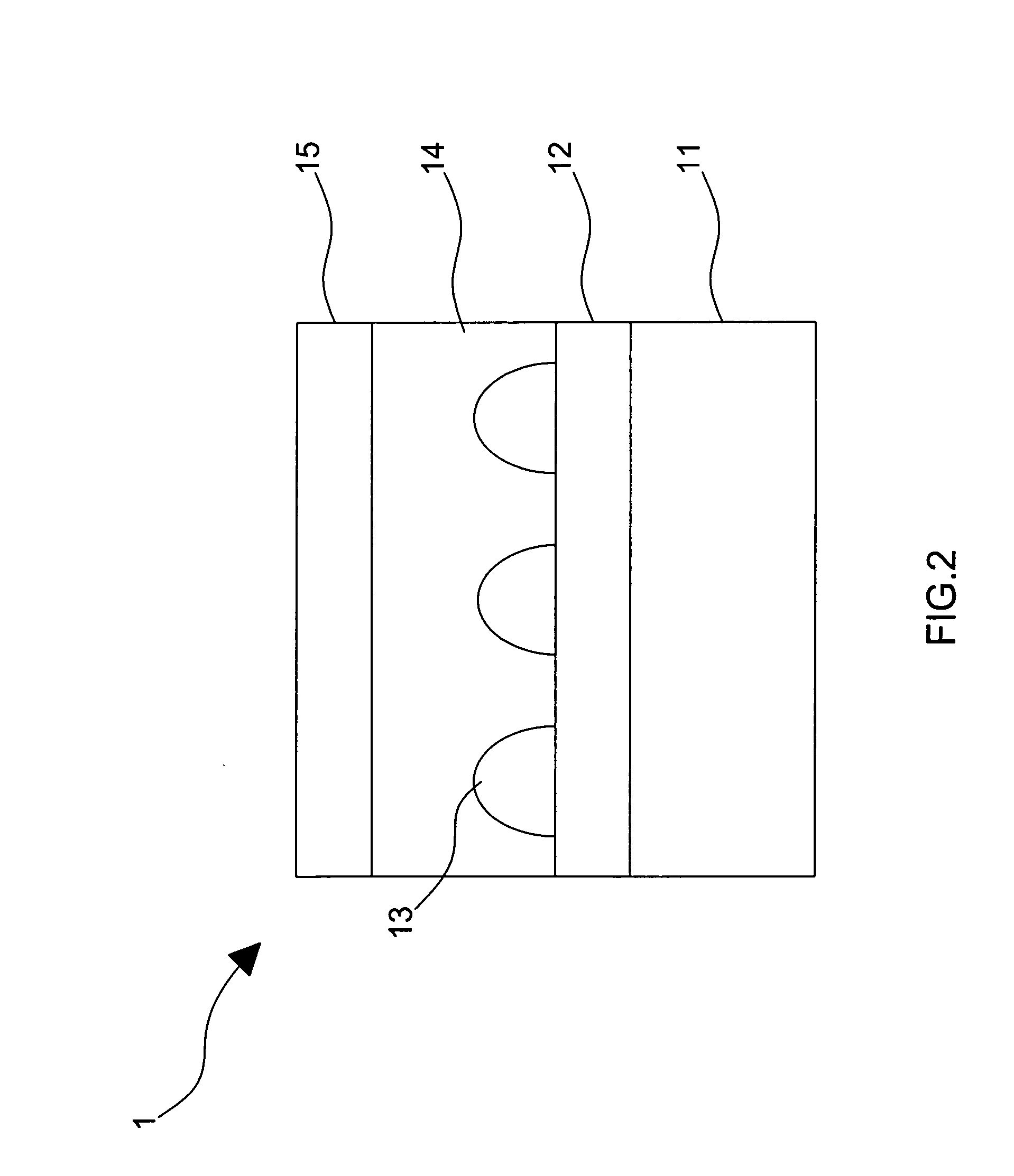
[0028]FIG. 4A is a schematic structure showing the second embodiment of this invention. As shown in the figure, a quantum dot optoelectronic device 1b comprises an epitaxy substrate 11b, an epitaxy buffer layer 12b, a quantum dot layer 13b, an overgrown layer 14b and a surface layer 14b, and a surface layer 15b, where the epitaxy substrate 11b, the epitaxy buffer layer 12b, and the surface layer 15b are made of GaAs; the quantum dot structure 13b is made of InAs; and the overgrown layer 14b is made of InAlAsSb.

[0029]FIG. 3B shows the room temperature photoluminescence spectra of the prior art 31, whose overgrown layer is InAlAs, and the second embodiment of this invention 32. The luminescence intensity of the quantum dot structure is obviously improved by the use of the InAlAsSb overgrown layer 14b because Sb serves as a surfactant that reduces the crystal defects in aluminum containing materials. Moreover, band gap of InAlAsSb is high enough so that the energy difference between th...


PUM


Abstract

A quantum dot optoelectronic device has an overgrown layer containing antimony (Sb). The optical characteristics and thermal stability of the optoelectronic device are thus greatly enhanced due to the improved crystal quality and carrier confinement of the quantum dot structure.

Description

FIELD OF THE INVENTION[0001]The present invention relates to an optoelectronic device; more particularly, relates to n quantum dot optoelectronic device having an overgrown layer containing antimony (Sb) to improve optical characteristics and thermal stability.DESCRIPTION OF THE RELATED ART(S)[0002]A general quantum dot optoelectronic device on a GaAs substrate is fabricated by covering a layer of InGaAs or InAlAs on quantum dots to improve size uniformity of quantum dots and to extend light emission wavelength after growing InAs quantum dots on a GaAs substrate. Yet, by doing so, the confinement potential of the carriers in quantum dot structure is lowered by the InGaAs; or, the light emission efficiency is reduced due to the poor crystal quality of InAlAs grown at low temperature. Besides, growing a heterostructure containing indium (In), like InGaAs or InAlAs, on a GaAs substrate may induce crystal defects if the lattice mismatch is too large, which adversely affect the performan...

Claims


Application Information

Patent Timeline
IPC IPC(8): H01L29/06
CPCB82Y10/00H01L29/127H01L29/20H01L33/06H01L33/32
Inventor LIU, WEI-SHENGCHYI, JEN-INN
Owner NAT CENT UNIV
Why Eureka
Try Eureka