

Semiconductor heterostructure, and preparation method and applications thereof
A heterogeneous structure and semiconductor technology, applied in semiconductor/solid-state device manufacturing, semiconductor devices, electrical components, etc., can solve problems that affect the quality of AlInN crystals and device performance, uneven material composition, fluctuations in In composition, etc., to achieve Achieve high-quality epitaxial growth, improve immiscibility, and eliminate reliability problems
- Summary
- Abstract
- Description
- Claims
- Application Information
AI Technical Summary
Problems solved by technology
Method used
Image

Examples
Embodiment 1
[0053] Embodiment 1 The Al contained in the device of this embodiment x In y Ga 1-x-y The N / GaN heterojunction can be fabricated as follows, where Al x In y Ga 1-x-y The specific composition of N is: aluminum component x=33%, indium component y=7%, gallium component 1-x-y=60%.
[0054] I. Non-pulse growth mode
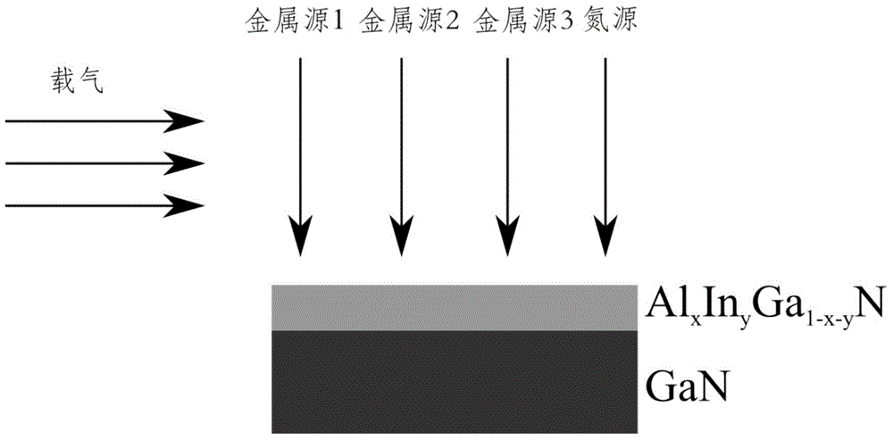
[0055] (1) GaN channel layer growth (assuming that the epitaxial growth of the nucleation layer, stress control layer, and buffer layer has been completed). The carrier gas is hydrogen, and the growth temperature is relatively high, 900-1200°C; the pressure of the reaction chamber is relatively high, 100-350mbar. The thickness of the GaN channel layer is more than 20nm, and the growth rate is 0.1-3μm / hr.
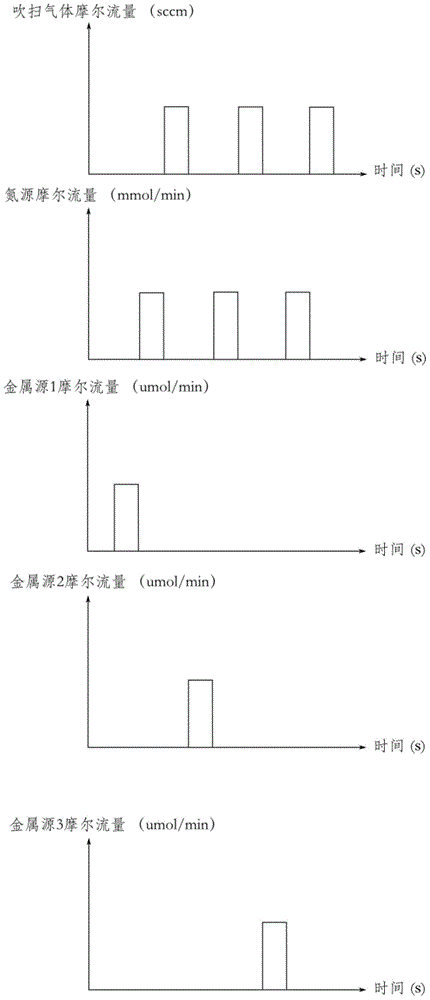
[0056] (2) Adjust the conditions of the reaction chamber to the growth conditions of the AlInGaN barrier layer. In the environment where ammonia (nitrogen source) is not turned off, the carrier gas is switched from hydrogen to nitrogen (or contains a small am...
Embodiment 2
[0063] Embodiment 2 The Al contained in the device of this embodiment x In y Ga 1-x-y The N / GaN heterojunction can be fabricated as follows, where Al x In y Ga 1-x-y The specific composition of N is: aluminum component x=66.01%, indium component y=13.99%, gallium component 1-x-y=20%
[0064]I. Non-pulse growth mode
[0065] (1) GaN channel layer growth (assuming that the epitaxial growth of the nucleation layer, stress control layer, and buffer layer has been completed). The carrier gas is hydrogen, and the growth temperature is relatively high, 900-1200°C; the pressure of the reaction chamber is relatively high, 100-350mbar. The thickness of the GaN channel layer is more than 20nm, and the growth rate is 0.1-3μm / hr.
[0066] (2) Adjust the conditions of the reaction chamber to the growth conditions of the AlInGaN barrier layer. In the environment where ammonia (nitrogen source) is not turned off, the carrier gas is switched from hydrogen to nitrogen (or contains a sma...
Embodiment 3
[0073] Embodiment 3 The Al contained in the device of this embodiment x In y Ga 1-x-y The N / GaN heterojunction can be fabricated as follows, where Al x In y Ga 1-x-y The specific composition of N is: aluminum component x=33.44%, indium component y=6.56%, gallium component 1-x-y=60%.
[0074] I. Non-pulse growth mode
[0075] (1) GaN channel layer growth (assuming that the epitaxial growth of the nucleation layer, stress control layer, and buffer layer has been completed). The carrier gas is hydrogen, and the growth temperature is relatively high, 900-1200°C; the pressure of the reaction chamber is relatively high, 100-350mbar. The thickness of the GaN channel layer is more than 20nm, and the growth rate is 0.1-3μm / hr.
[0076] (2) Adjust the conditions of the reaction chamber to the growth conditions of the AlInGaN barrier layer. In the environment where ammonia (nitrogen source) is not turned off, the carrier gas is switched from hydrogen to nitrogen (or contains a sm...
PUM
| Property | Measurement | Unit |
|---|---|---|
| thickness | aaaaa | aaaaa |
Abstract
Description
Claims
Application Information