Epitaxial film forming method, sputtering apparatus, manufacturing method of semiconductor light-emitting element, semiconductor light-emitting element, and illumination device

a manufacturing method and film technology, applied in the direction of polycrystalline material growth, chemically reactive gas growth, crystal growth process, etc., can solve the problems of not revealing a control method, unable to obtain high-quality gan film, and unable to obtain favorable emission characteristics, etc., to achieve the effect of improving the light emission characteristics of light-emitting elements such as led and ld

Inactive Publication Date: 2013-10-24
CANON ANELVA CORP
View PDF4 Cites 7 Cited by
  • Summary
  • Abstract
  • Description
  • Claims
  • Application Information

AI Technical Summary

Benefits of technology

[0025]According to the present invention, an epitaxial film of a group III nitride semiconductor in which mosaic expansion of tilt or twist is small, mixture of +c polarity and −c polarity is reduced, and unification of the +c polarity is improved can be fabricated on the α—Al2O3 substrate by using the sputtering method. Moreover, by using the group III nitride semiconductor epitaxial film fabricated by this sputtering method, light emission characteristics of light-emitting elements such as LED and LD can be improved.

Problems solved by technology

However, the prior-art technologies do not disclose a method of controlling polarity, and there is a serious problem in employing the sputtering method as a manufacturing process of a group III nitride semiconductor.
Moreover, when a GaN film was grown on the AlN film in which the +c polarity and the −c polarity were mixed by the MOCVD method, a high-quality GaN film could not be obtained.
Moreover, a light-emitting element was fabricated by using the obtained GaN film, but favorable emission characteristics could not be obtained.

Method used


Image

  • Epitaxial film forming method, sputtering apparatus, manufacturing method of semiconductor light-emitting element, semiconductor light-emitting element, and illumination device
  • Epitaxial film forming method, sputtering apparatus, manufacturing method of semiconductor light-emitting element, semiconductor light-emitting element, and illumination device
  • Epitaxial film forming method, sputtering apparatus, manufacturing method of semiconductor light-emitting element, semiconductor light-emitting element, and illumination device

Examples


example

First Example

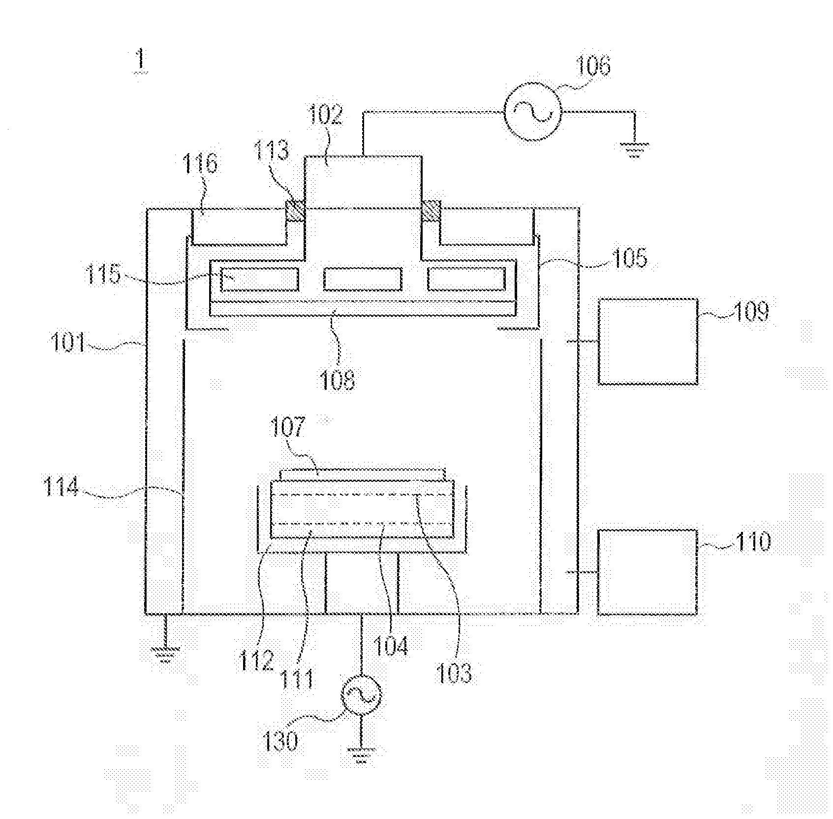
[0099]As a first example of the present invention, an example in which an AlN film as the buffer layer 602 (See FIG. 6) was formed on an α—Al2O3 (0001) substrate by using the film-forming method of a group III nitride semiconductor thin film according to an embodiment of the present invention will be described. More specifically, an example in which, in a state where the high-frequency bias power was applied to the bias electrode 103, the AlN film was formed on the α—Al2O3 (0001) substrate by using the sputtering method will be described. In the first example, the AlN film was formed by using the sputtering apparatus similar to that in FIG. 1. Moreover, the frequencies of the high-frequency power to be applied to the target electrode 102 and the high-frequency power to be applied to the bias electrode 103 are set to 13.56 MHz and 13.54 MHz, respectively.

[0100]In the first example, first, the α—Al2O3 (0001) substrate was conveyed to the vacuum vessel 101 maintained at 1×...

second example

[0110]Subsequently, as a second example of the present invention, an example in which the AlN film fabricated by using the film-forming method of the group III nitride semiconductor thin film according to the present invention was used as a buffer layer and an undoped GaN film as the group III nitride semiconductor intermediate layer 603 in FIG. 6 was formed on the buffer layer by using the MOCVD method will be described.

[0111]The AlN film was formed on the α—Al2O3 (0001) substrate by using the sputtering method with the same apparatus and conditions as those in the first example and then, a wafer (substrate) was introduced into the MOCVD device so as to form an undoped GaN film having a film thickness of 5 μm.

[0112]The surface of the obtained undoped GaN film was a mirror surface, and it was indicated in the XRD measurement in the 2θ / ω scan mode at a symmetric reflection position that the undoped GaN film had a c-axis orientation. Subsequently, the XRC measurement in the ω scan mod...

third example

[0115]As a third example of the present invention, an example will be described in which the AlN film fabricated by using the film-forming method of the group III nitride semiconductor thin film according to the present invention was used as a buffer layer, and on the buffer layer, by using the MOCVD method, the group III nitride semiconductor intermediate layer made of undoped GaN, the n-type group III nitride semiconductor layer made of Si doped GaN, the group III nitride semiconductor active layer having an MQW structure of InGaN and GaN, and the p-type group III nitride semiconductor layer made of Mg doped GaN were epitaxially grown sequentially and moreover, after the n-type electrode layer, the translucent electrode, the p-type electrode layer, and the protective film were formed, a wafer was separated by scribing and an LED element was fabricated.

[0116]By using the sputtering method, the AlN film as the buffer layer 602 was formed on the α—Al2O3 (0001) substrate under the sam...


PUM

PropertyMeasurementUnit
frequencyaaaaaaaaaa
frequencyaaaaaaaaaa
frequencyaaaaaaaaaa

Abstract

The present invention provides an epitaxial film forming method for epitaxially growing a high-quality group III nitride semiconductor thin film on an α—Al2O3 substrate by a sputtering method. In the epitaxial film forming method according to an embodiment of the present invention, when an epitaxial film of a group III nitride semiconductor thin film is to be formed on the α—Al2O3 substrate arranged on a substrate holder provided with a heater electrode and a bias electrode of a sputtering apparatus, in a state where the α—Al2O3 substrate is maintained at a predetermined temperature by the heater electrode, high-frequency power is applied to a target electrode and high-frequency bias power is applied to a bias electrode and at that time, the powers are applied so that frequency interference between the high-frequency power and the high-frequency bias power does not occur.

Description

CROSS-REFERENCE TO RELATED APPLICATIONS[0001]This application is a continuation application of International Application No. PCT / JP2011 / 007040, filed Dec. 16, 2011, which claims the benefit of Japanese Patent Application No. 2010-289265, filed Dec. 27, 2010. The contents of the aforementioned applications are incorporated herein by reference in their entireties.TECHNICAL FIELD[0002]The present invention relates to an epitaxial film forming method, a sputtering apparatus, a manufacturing method of a semiconductor light-emitting element, a semiconductor light-emitting element, and an illumination device and particularly to an epitaxial film forming method capable of forming a high-quality epitaxial film, a manufacturing method of a semiconductor light-emitting element using such epitaxial film, a sputtering apparatus, a semiconductor light-emitting element, and an illumination device.BACKGROUND ART[0003]Group III nitride semiconductors are compound semiconductor materials of an alumin...

Claims


Application Information

Patent Timeline
Patent Type & Authority Applications(United States)
IPC IPC(8): H01L21/02
CPCH01L21/02631C23C14/0617C23C14/345C30B23/005C30B23/02C30B25/06C30B29/403H01L21/0242H01L21/02458H01L21/0254H01L33/007H01L21/203H01L33/32
Inventor DAIGO, YOSHIAKIISHIBASHI, KEIJI
Owner CANON ANELVA CORP
Why Eureka
Try Eureka