Semiconductor device and method of manufacturing the same

a technology of semiconductors and semiconductors, applied in the direction of semiconductor devices, electrical equipment, transistors, etc., can solve problems such as deterioration or operating errors of electrical characteristics, and achieve the effect of improving electrical characteristics and reliability of devices

Active Publication Date: 2013-10-24
SK HYNIX INC
View PDF2 Cites 21 Cited by
  • Summary
  • Abstract
  • Description
  • Claims
  • Application Information

AI Technical Summary

Benefits of technology

[0006]An embodiment relates to a semiconductor device that can improve electrical characteristics and reliability of a device and a method of manufacturing the same.

Problems solved by technology

With increasing integration degree of devices, device size and spacing between devices become smaller, which may result in operating errors or deterioration of electrical characteristics due to interference between the devices.

Method used


Image

  • Semiconductor device and method of manufacturing the same
  • Semiconductor device and method of manufacturing the same
  • Semiconductor device and method of manufacturing the same

Examples


Embodiment Construction

[0015]Hereinafter, various exemplary embodiments of the present disclosure will be described in detail with reference to the accompanying drawings. The figures are provided to enable those of ordinary skill in the art to make and use the present invention according to the embodiments of the present invention.

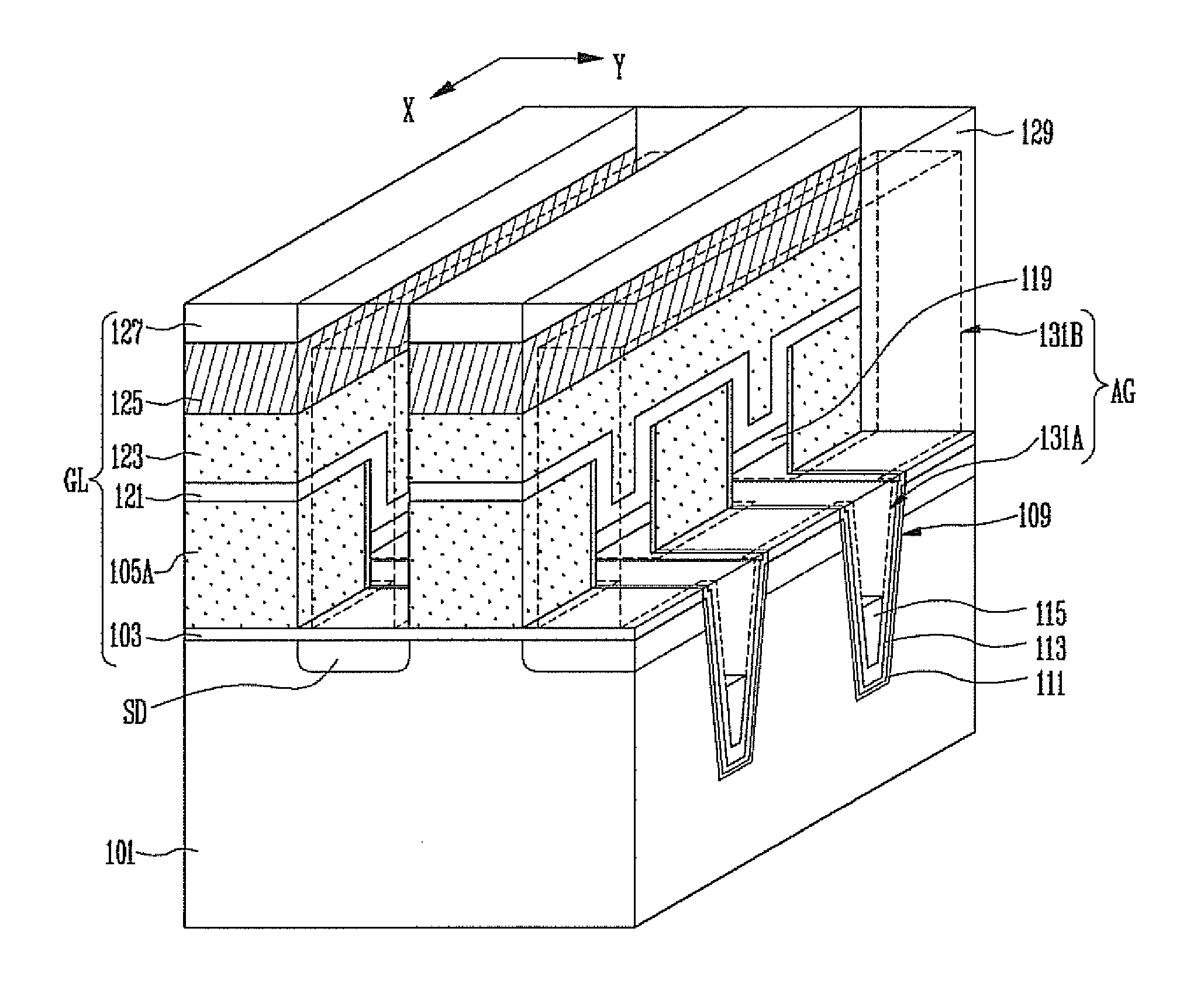
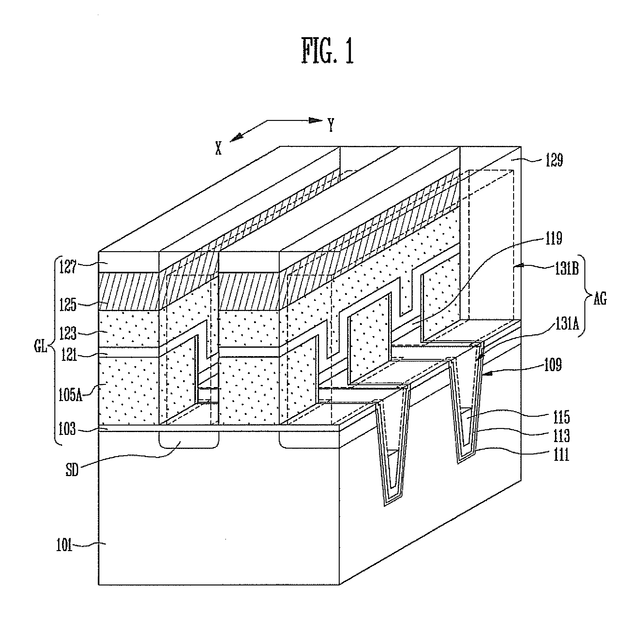
[0016]FIG. 1 is a three-dimensional view of a semiconductor device according to an embodiment of the present invention.

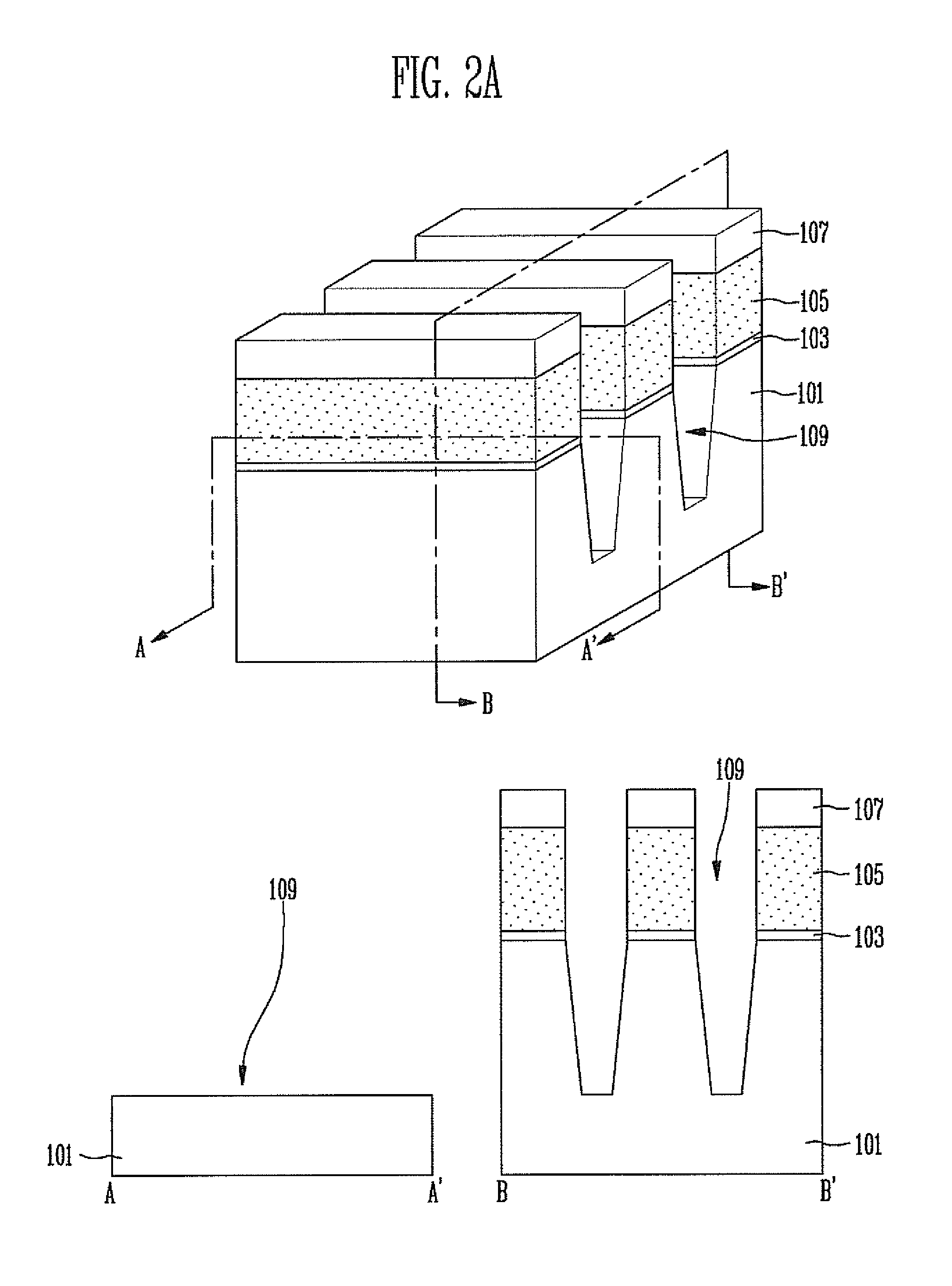
[0017]Referring to FIG. 1, a plurality of trenches 109 may be formed in isolation regions of a semiconductor substrate 101 in a first direction Y. Active regions may be defined between the isolation regions. In addition, gate lines GL may be arranged in a second direction X crossing the trenches 109. More specifically, the gate lines GL may be formed over the semiconductor substrate 101 in the second direction X such that the gate lines GL may cross the active regions and the isolation regions of the semiconductor substrate 101. Source / drains SD may be formed in...


PUM


Abstract

A semiconductor device includes a semiconductor substrate having a plurality of isolation regions, a plurality of trenches, where each of the plurality of trenches is formed in a corresponding isolation region, of the plurality of isolation regions, and where the plurality of trenches are arranged, in parallel, along a first direction, a plurality of gate lines formed on the semiconductor substrate in a second direction crossing the plurality of trenches, an insulating layer formed between each of the plurality of gate lines, a first air gap formed in at least one of the plurality of trenches, the first air gap extending in the first direction, and a second air gap formed in at least one of the insulating layers, the second air gap extending in the second direction.

Description

CROSS-REFERENCE TO RELATED APPLICATION[0001]Priority is claimed to Korean patent application number 10-2012-0041518, filed on Apr. 20, 2012, the entire disclosure of which is incorporated herein by reference in its entirety.BACKGROUND[0002]1. Field of Invention[0003]Embodiments of the present invention relate to a semiconductor device and a method of manufacturing the same and, more particularly, to a semiconductor device including an isolation region and a method of manufacturing the same.[0004]2. Description of Related Art[0005]With increasing integration degree of devices, device size and spacing between devices become smaller, which may result in operating errors or deterioration of electrical characteristics due to interference between the devices.BRIEF SUMMARY[0006]An embodiment relates to a semiconductor device that can improve electrical characteristics and reliability of a device and a method of manufacturing the same.[0007]A semiconductor device according to an exemplary e...

Claims


Application Information

Patent Timeline
Patent Type & Authority Applications(United States)
IPC IPC(8): H01L29/788H01L29/06H01L21/762
CPCH01L21/764H10B41/43
Inventor JUNG, WOO DUCKKIM, SUNG SOONSONG, JU IL
Owner SK HYNIX INC
Why Eureka
Try Eureka