Semiconductor device having calibration circuit that adjusts impedance of output buffer

a technology of output buffer and calibration circuit, which is applied in the direction of logic circuits, reliability increasing modifications, coupling arrangements of logic circuits, etc., can solve the problems of taking a long time to perform calibration operations, and not being able to complete calibration operations in a predetermined time period. , to achieve the effect of shortening the time of calibration operation

Active Publication Date: 2013-10-24
LONGITUDE LICENSING LTD
View PDF6 Cites 5 Cited by
  • Summary
  • Abstract
  • Description
  • Claims
  • Application Information

AI Technical Summary

Benefits of technology

[0012]According to the present invention, because first and second control codes can be generated in parallel, a calibration operation can be completed in a shorter time. Therefore, even when the frequency of a clock signal to be used is high or the number of bits of a control code is large, it is possible to correctly complete the calibration operation within a predetermined time period.

Problems solved by technology

Therefore, there has been a problem that it takes a long time to perform a calibration operation.
Therefore, in some cases, the calibration operation may not be completed correctly.
However, particularly in the semiconductor devices described in Japanese Patent Application Laid-open Nos. 2008-219865 and 2008-228276, the calibration operation may not be completed within a predetermined time period if the number of bits of the impedance code is increased.

Method used


Image

  • Semiconductor device having calibration circuit that adjusts impedance of output buffer
  • Semiconductor device having calibration circuit that adjusts impedance of output buffer
  • Semiconductor device having calibration circuit that adjusts impedance of output buffer

Examples


first embodiment

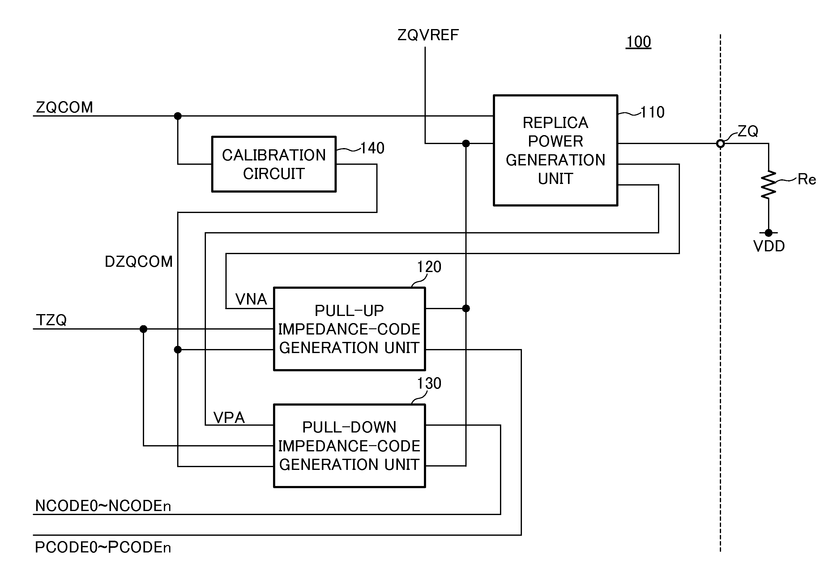
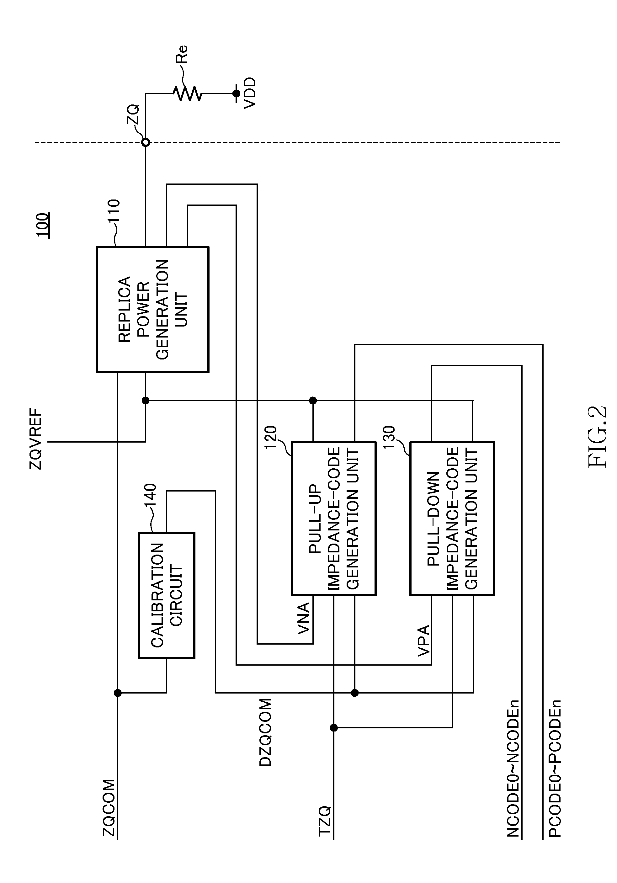
[0042]Turning to FIG. 2, the calibration circuit 100 according to the present invention includes a replica power generation unit 110, a pull-up impedance-code generation unit 120, and a pull-down impedance-code generation unit 130. The replica power generation unit 110 is a circuit that generates bias potentials VNA and VPA, which are control signals, based on the reference potential ZQVREF. The bias potential VNA is supplied to the pull-up impedance-code generation unit 120, and the bias potential VPA is supplied to the pull-down impedance-code generation unit 130. Although these units 110, 120, and 130 are activated based on the calibration signal ZQCOM, in order to secure a time for the bias potentials VNA and VPA to be stabilized, the pull-up impedance-code generation unit 120 and the pull-down impedance-code generation unit 130 are activated in response to the calibration signal ZQCOM that is delayed by a delay circuit 140.

[0043]Turning to FIG. 3, the replica power generation u...

second embodiment

[0064]the present invention is explained next with reference to FIGS. 8 to 12.

[0065]As shown in FIG. 9, the calibration circuit 100 according to the second embodiment includes a pull-up impedance-code generation unit 160 and a pull-down impedance-code generation unit 170. In the second embodiment, the delay circuit 140 and the replica power generation unit 110 shown in FIG. 2 are not included in the calibration circuit 100. Therefore, the calibration circuit 100 according to the second embodiment has characteristics such that its circuit size is smaller and the current consumption is also smaller as compared to the calibration circuit 100 according to the first embodiment.

[0066]Turning to FIG. 10, the pull-up impedance-code generation unit 160 has a circuit configuration similar to that of the pull-up impedance-code generation unit 120 shown in FIG. 5, including an impedance adjustment unit 161 that is connected between the power supply line to which the power supply potential VDD i...


PUM


Abstract

Disclosed herein is a device that includes: a data terminal; an output buffer coupled to the data terminal, the output buffer including a first output unit having a plurality of first output transistors of a first conductivity type and a second output unit having a plurality of second output transistors of a second conductivity type; and a calibration circuit including a first code generation unit that generates a first control code that controls an impedance of the first output unit by performing a first calibration operation based on an impedance of a first reference unit and a second code generation unit that generates a second control code that controls an impedance of the second output unit by performing a second calibration operation based on an impedance of a second reference unit. The calibration circuit performs the first and second calibration operations in parallel.

Description

BACKGROUND OF THE INVENTION[0001]1. Field of the Invention[0002]The present invention relates to a semiconductor device, and more particularly relates to a semiconductor device including a calibration circuit that adjusts an impedance of an output buffer.[0003]2. Description of Related Art[0004]In a semiconductor device such as a DRAM (Dynamic Random Access Memory), a calibration circuit that adjusts an impedance of an output buffer is employed in some cases (see Japanese Patent Application Laid-open Nos. 2008-219865 and 2008-228276). The output buffer includes a pull-up output unit and a pull-down output unit, and the impedance of these units is respectively controlled based on a pull-up impedance code and a pull-down impedance code generated by the calibration circuit.[0005]However, in the semiconductor devices described in Japanese Patent Application Laid-open Nos. 2008-219865 and 2008-228276, the pull-up impedance code is generated first, and then the pull-down impedance code is...

Claims


Application Information

Patent Timeline
Patent Type & Authority Applications(United States)
IPC IPC(8): H03K19/0175
CPCH03K19/017545
Inventor MATANO, TATSUYA
Owner LONGITUDE LICENSING LTD
Why Eureka
Try Eureka