Semiconductor wafer and method for auto-calibrating integrated circuit chips using pll at wafer level

a technology of integrated circuit chips and semiconductor wafers, applied in the direction of automatic control, instruments, computing, etc., can solve the problems of high failure probability, increased chip area, and inability to completely uniformize radio frequency/analog chip performance, so as to reduce the inferiority rate and accelerate the the effect of rapid calibration of integrated circuit chip performan

Inactive Publication Date: 2013-10-24
ELECTRONICS & TELECOMM RES INST
View PDF2 Cites 1 Cited by
  • Summary
  • Abstract
  • Description
  • Claims
  • Application Information

AI Technical Summary

Benefits of technology

[0009]The present invention has been made in an effort to provide a method of auto-calibrating integrated circuit chips at a wafer level having advantages of rapidly calibrating performance of integrated circuit chips at a wafer level. In general, when adjusting performance of a circuit that outputs a digital value, performance of a plurality of integrated circuit chips can be rapidly calibrated, and an inferiority rate can be reduced. Therefore, by calibrating a frequency that is generated in an operation frequency generator that outputs a digital value rather than calibrating performance of a bias circuit that outputs an analog value, it is reasonable to calibrate the performance of all the integrated circuit chips. The present invention has been made in an effort to further provide a method of auto-calibrating integrated circuit chips at a wafer level having advantages of auto-calibrating an operation frequency of integrated circuit chips at a wafer level using a PLL.

Problems solved by technology

In general, a chip that is formed with only a digital logic circuit is less influenced by a process change, but a radio frequency (RF) / analog chip including many passive elements is influenced by a process change and thus the radio frequency (RF) / analog chip does not have completely uniform performance.
Particularly, in tag chips that are used for RFID, in an operation frequency generation circuit using a capacitor element or in a bias circuit using a resistor element, a failure occurrence probability is high.
However, in laser trimming technology, time is additionally consumed, and when a calibration circuit is added, there is a drawback that an area of a chip increases and thus it is difficult to apply the above technology for mass production of super-cheap tag chips.
However, the method of testing an RFID tag chip with an on-wafer is a method of verifying only whether a tag chip is defective, and in the method of calibrating performance of a tag using a one-time programmable memory, a relatively large amount of time is consumed in performance calibration of an individual tag chip and thus there is a problem that the production cost of the tag increases.

Method used


Image

  • Semiconductor wafer and method for auto-calibrating integrated circuit chips using pll at wafer level
  • Semiconductor wafer and method for auto-calibrating integrated circuit chips using pll at wafer level
  • Semiconductor wafer and method for auto-calibrating integrated circuit chips using pll at wafer level

Examples


Embodiment Construction

[0019]In the following detailed description, only certain exemplary embodiments of the present invention have been shown and described, simply by way of illustration. As those skilled in the art would realize, the described embodiments may be modified in various different ways, all without departing from the spirit or scope of the present invention. Accordingly, the drawings and description are to be regarded as illustrative in nature and not restrictive. Like reference numerals designate like elements throughout the specification.

[0020]In addition, in the entire specification and claims, unless explicitly described to the contrary, the word “comprise” and variations such as “comprises” or “comprising” will be understood to imply the inclusion of stated elements but not the exclusion of any other elements.

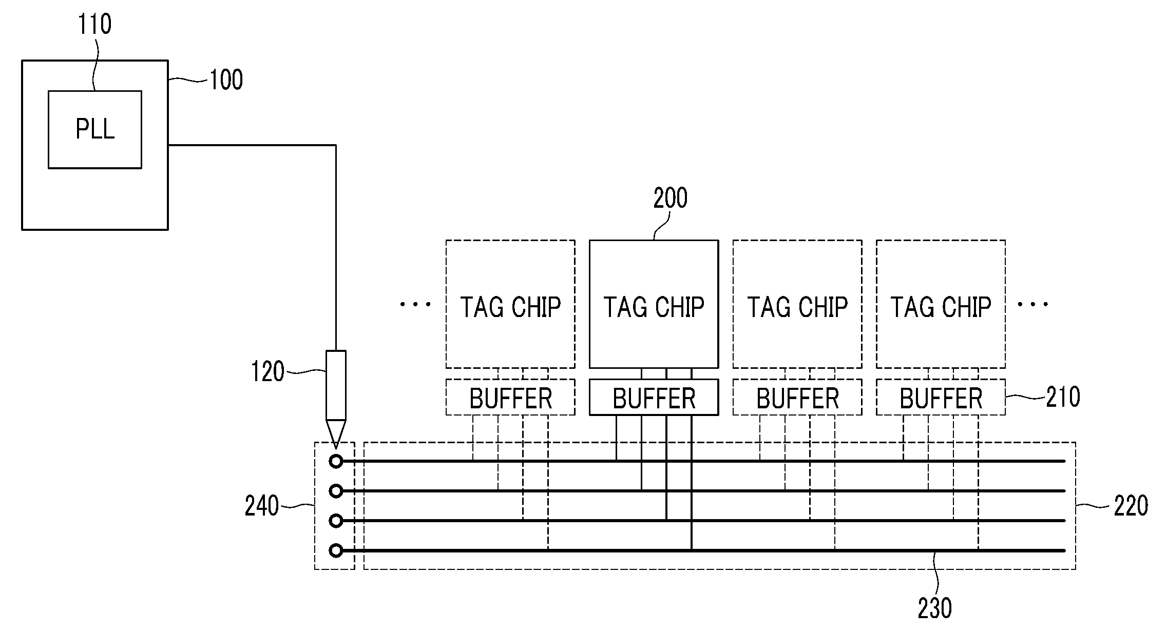
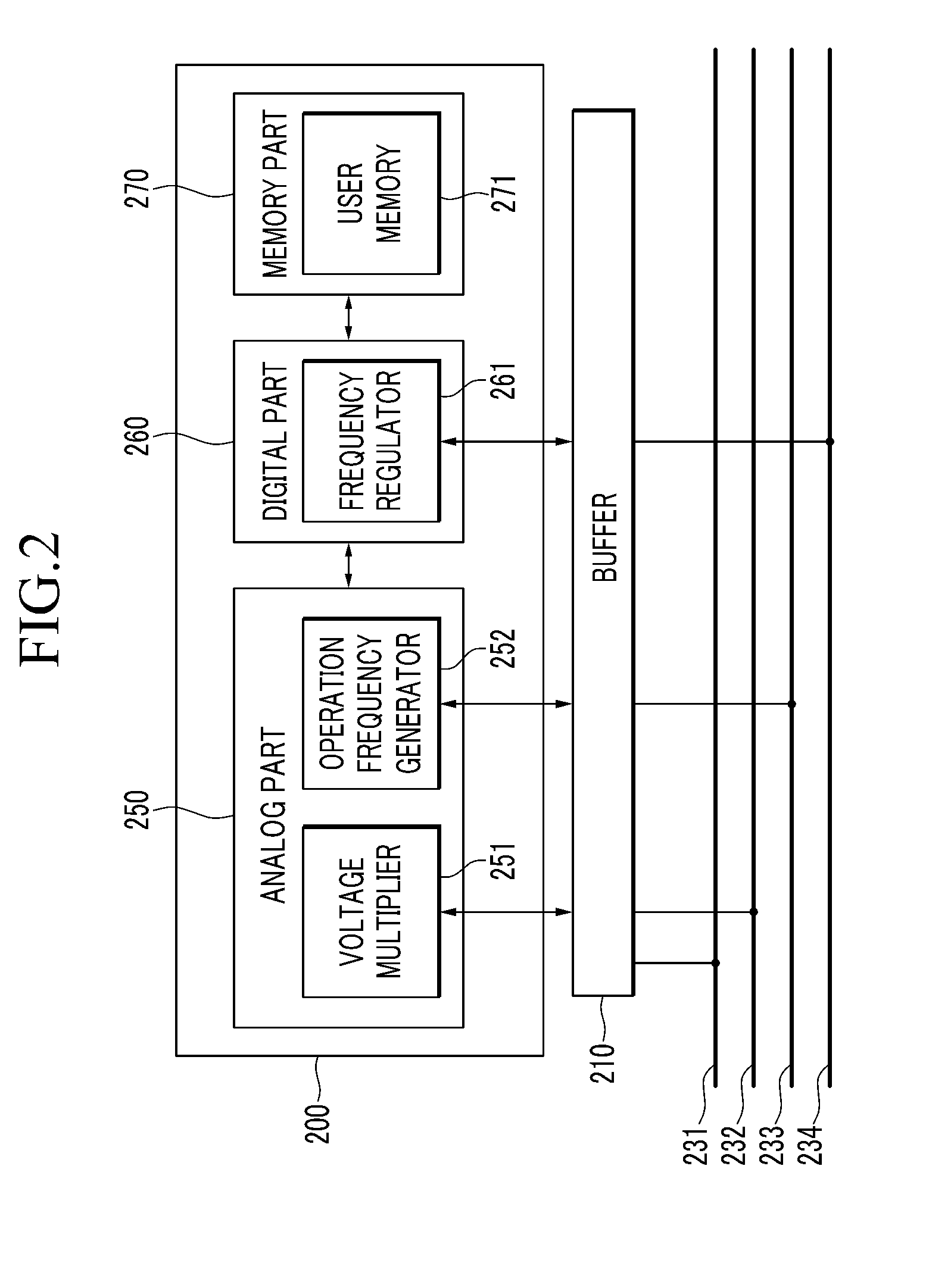
[0021]Hereinafter, a method of auto-calibrating integrated circuit chips of a wafer level according to an exemplary embodiment of the present invention will be described in detail ...


PUM


Abstract

In integrated circuit chips that are used for RFID, a method of calibrating an operation frequency that is generated in an operation frequency generator and a semiconductor wafer including a calibration circuit are provided. The method of calibrating an operation frequency of integrated circuit chips includes: supplying DC power to the integrated circuit chips; selecting an integrated circuit chip to perform calibration of an operation frequency; receiving an operation frequency that is generated in the selected integrated circuit chip; calculating a difference between a phase of the operation frequency and a phase of a calibration target frequency; generating a frequency calibration value of the operation frequency using the phase difference; transmitting a control signal including the frequency calibration value to the integrated circuit chip; and releasing a selection of the integrated circuit chip in which calibration of the operation frequency is complete.

Description

CROSS-REFERENCE TO RELATED APPLICATION[0001]This application claims priority to and the benefit of Korean Patent Application No. 10-2012-0042305 filed in the Korean Intellectual Property Office on Apr. 23, 2012, the entire contents of which are incorporated herein by reference.BACKGROUND OF THE INVENTION[0002](a) Field of the Invention[0003]The present invention relates to a method of auto-calibrating integrated circuit chips at a wafer level. More particularly, the present invention relates to a method of auto-calibrating integrated circuit chips in order to uniformly improve performance of integrated circuit chips that are used for radio frequency identification (referred to as an ‘RFID’) or an ubiquitous sensor network (referred to as an ‘USN’) at a wafer level using a phase-locked loop (PLL).[0004](b) Description of the Related Art[0005]In general, RFID is technology that stores information at a tag that is formed in a form of integrated circuit chips or reads the stored informa...

Claims


Application Information

Patent Timeline
Patent Type & Authority Applications(United States)
IPC IPC(8): H03L7/06
CPCG06K19/0722G06K19/0726G06K19/07H03L7/00
Inventor KIM, HYUNSEOKCHOI, SU NALEE, HEYUNG SUBPYO, CHEOL SIG
Owner ELECTRONICS & TELECOMM RES INST
Why Eureka
Try Eureka