Method and Apparatus for the Line Narrowing of Diode Lasers

Inactive Publication Date: 2013-10-31
TRANSLITH SYST
View PDF4 Cites 0 Cited by
  • Summary
  • Abstract
  • Description
  • Claims
  • Application Information

AI Technical Summary

Problems solved by technology

As shown in FIG. 1, this approach also adds considerable size to each diode laser

Method used


Image

  • Method and Apparatus for the Line Narrowing of Diode Lasers
  • Method and Apparatus for the Line Narrowing of Diode Lasers
  • Method and Apparatus for the Line Narrowing of Diode Lasers

Examples


Embodiment Construction

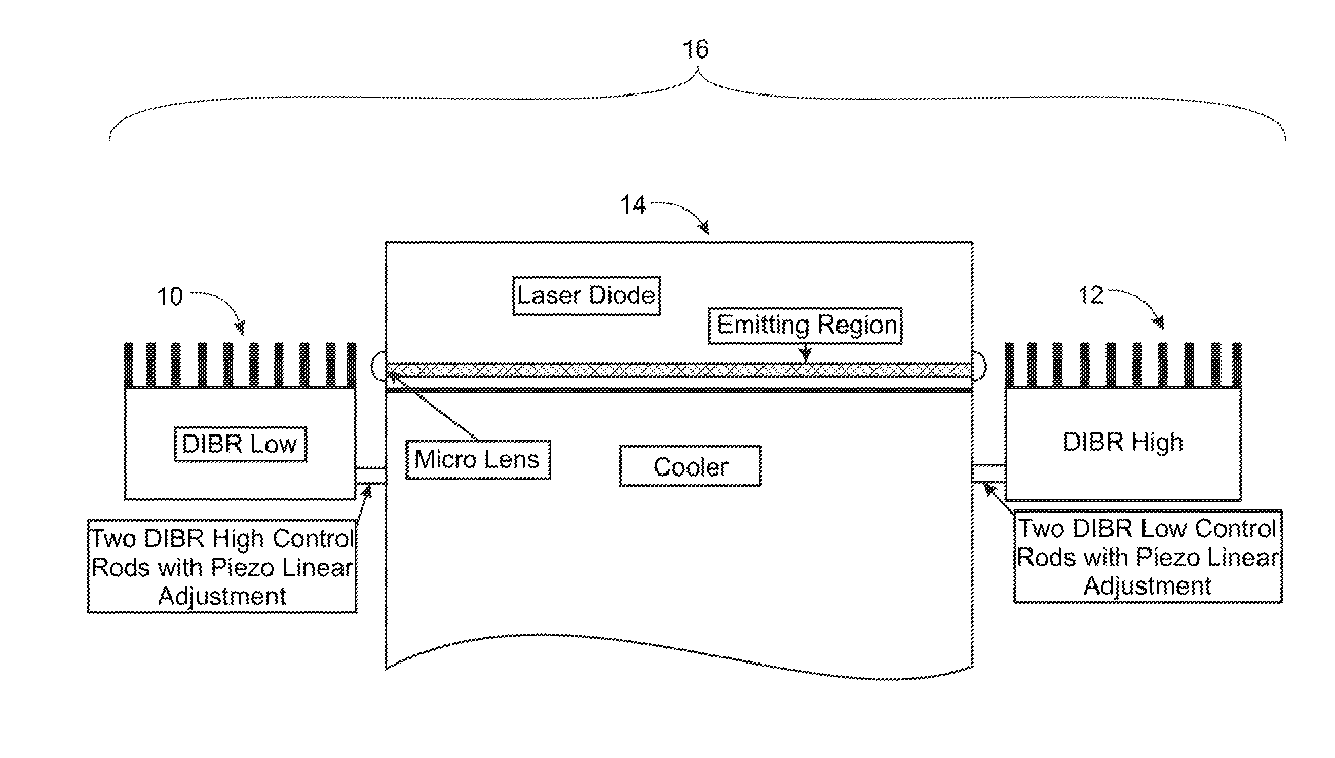
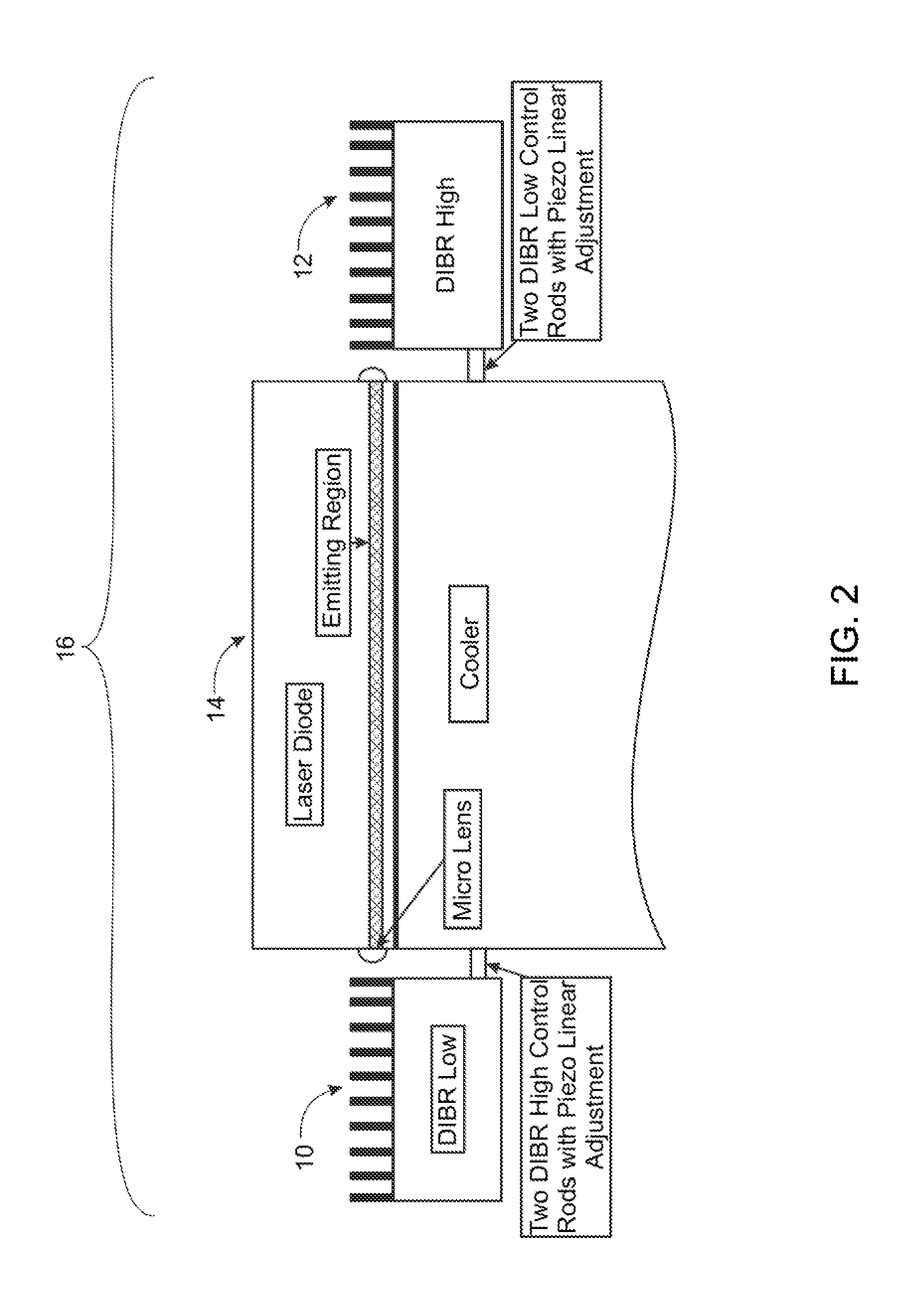
[0020]The present invention is a method and apparatus for the line narrowing of diode lasers. As shown in FIG. 2, two dielectric stacks 10, 12 are used together with a diode laser 14 to form a laser cavity 16 with the dielectric stacks at opposite ends of the laser cavity. The upper band edge of the bandpass reflector of one of the dielectric stacks 10 (the “DIBR low structure”) is matched with the lower band edge of the bandpass reflector of the other dielectric stack 12 (the “DIBR high structure”).

[0021]The dielectric stacks are comprised of air and a dielectric material with a low coefficient of thermal expansion (“CTE”). The dielectric stacks are fabricated using controlled laser ablation of the dielectric material.

[0022]In a preferred embodiment, the dielectric stack combination creates a bandpass reflector at a design center wavelength. The thickness of the materials in the dielectric stack is measured in multiples of the Quarter Wave Optical Thickness (QWOT). The optical refl...


PUM

PropertyMeasurementUnit
Timeaaaaaaaaaa
Nanoscale particle sizeaaaaaaaaaa

Abstract

A system for narrowing the spectral output of diode lasers through the use of dielectric stacks in the laser cavity comprising an alternating sequence of layers of dielectric material and air, which dielectric stacks are fabricated through the controlled laser ablation of the dielectric material.

Description

CROSS-REFERENCE TO RELATED APPLICATIONS [0001]The present application claims the benefit of U.S. Provisional Patent Application No. 61 / 619,388 filed on Apr. 2, 2012, and is a continuation-in-part of U.S. patent application Ser. No. 12 / 800,554 filed on May 17, 2010, which claims the benefit of U.S. Provisional Patent Application No. 61 / 216,306 filed on May 15, 2009, all of which are incorporated herein by reference.TECHNICAL FIELD OF THE INVENTION [0002]The present invention relates to a method and apparatus for the line narrowing of a diode laser. More specifically, it relates to a method and apparatus for the line narrowing of a diode laser with an integrated Bragg reflector fabricated using controlled laser ablation.BACKGROUND OF THE INVENTION [0003]Diode lasers notionally operate in the 800 nm range with a ˜2 nm wide spectral output. Many applications such as diode pumped alkali lasers (“DPALs”) require spectral outputs of diode lasers to be reduced to the ˜0.5 nm range or less.[...

Claims


Application Information

Patent Timeline
IPC IPC(8): H01S5/20B23K26/36
CPCH01S5/20B23K26/367H01S3/1055H01S5/0267H01S5/141G02B5/285B23K26/364
Inventor HOFF, PAULRONNING, DONALD
Owner TRANSLITH SYST
Why Eureka
Try Eureka