Mounting structure for circuit component and method for mounting circuit component

a technology for mounting structures and circuit components, applied in the direction of printed circuit aspects, electrical apparatus construction details, printed circuit non-printed electric components association, etc., can solve the problems of easy vibration of circuit components mounted on the circuit board, etc., to prevent abnormal noise

Inactive Publication Date: 2013-10-31
PANASONIC CORP
View PDF4 Cites 1 Cited by
  • Summary
  • Abstract
  • Description
  • Claims
  • Application Information

AI Technical Summary

Benefits of technology

[0014]In mounting a relatively large circuit component such as an electrolytic capacitor and a film capacitor on a circuit board, the structure above decreases a protruding height of the component, preventing abnormal noise caused by making contact the circuit component with the circuit board.
[0020]In mounting a relatively large circuit component such as an electrolytic capacitor and a film capacitor on the circuit board, the method above allows such a component to have decrease in a protruding height of the component beyond the circuit board, preventing abnormal noise caused by making contact the circuit component with the circuit board.

Problems solved by technology

In a plasma display apparatus, a circuit component mounted on the circuit board often has a vibration caused by vibrations occurred outside the plasma display apparatus.
Particularly, a plasma display apparatus having a large screen—where the apparatus itself and the circuit boards have increase in size—is easily affected by vibrations occurred outside the plasma display apparatus.
As a result, this develops a new problem that circuit components mounted on the circuit board easily vibrate.
Among others, in a plasma display apparatus with a built-in speaker, the increase in size further increases the tendency of the circuit components to vibrate.
Therefore, when such a relatively large circuit component has vibrations and contacts with the circuit board, abnormal noise can occur.

Method used


Image

  • Mounting structure for circuit component and method for mounting circuit component
  • Mounting structure for circuit component and method for mounting circuit component
  • Mounting structure for circuit component and method for mounting circuit component

Examples


first exemplary embodiment

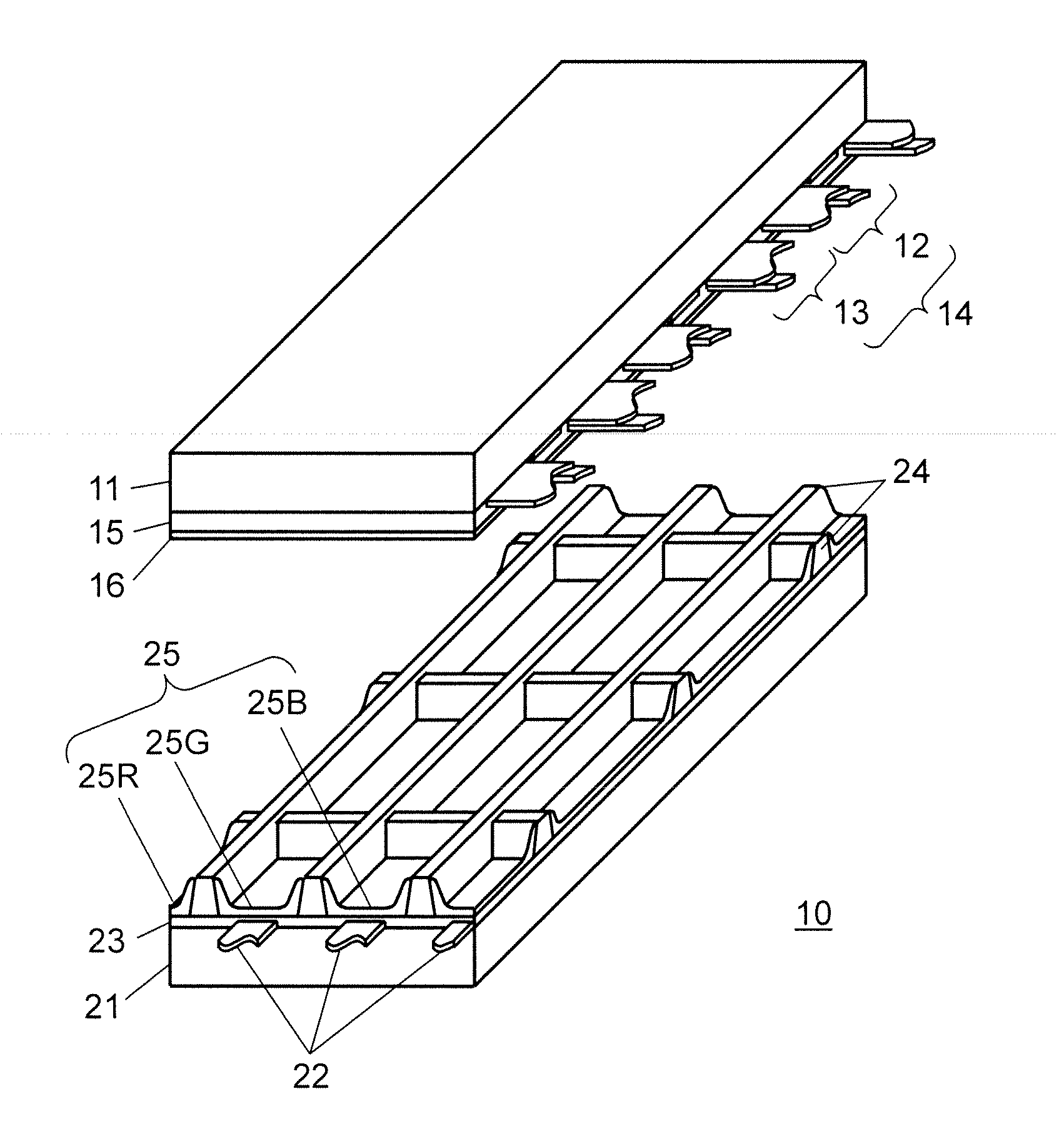
[0038]FIG. 1 is an exploded perspective view showing the structure of panel 10 for use in a plasma display apparatus in accordance with the first exemplary embodiment of the present invention.

[0039]A plurality of display electrode pairs 14, each including scan electrode 12 and sustain electrode 13, is formed on front substrate 11 made of glass. Dielectric layer 15 is formed so as to cover scan electrodes 12 and sustain electrodes 13. Protective layer 16 is formed over dielectric layer 15.

[0040]Protective layer 16 is made of a material predominantly composed of magnesium oxide (MgO). The MgO-based material is proven as being effective in decreasing a discharge start voltage in the discharge cells. Besides, the material offers a large coefficient of secondary electron emission and high durability against a gas of neon (Ne) xenon (Xe) used as discharge gas.

[0041]Protective layer 16 may be a single-layer structure or a multi-layer structure. Besides, protective layer 16 may be formed of...

second exemplary embodiment

[0088]FIG. 5A is a plan view showing an example of opening 42 formed in circuit board 41 of plasma display apparatus 30 in accordance with the second exemplary embodiment of the present invention.

[0089]FIG. 5B is a plan view schematically showing an example of the mounting structure after the completion of mounting electrolytic capacitor 52 on circuit board 41 of plasma display apparatus 30 in accordance with the second exemplary embodiment of the present invention.

[0090]As is shown in FIG. 5A, circuit board 41 has opening 42, through-hole 43, and protrusion 45.

[0091]Opening 42 is formed in circuit board 41 so as to have a size larger than the external dimensions of body 52a except for lead wire 53 of electrolytic capacitor 52 to be mounted on circuit board 41.

[0092]Through-hole 43 is formed in circuit board 41 so as to let lead wire 53 of electrolytic capacitor 52 through.

[0093]Protrusion 45 is formed on one side of opening 42 and has a shape protruding from the one side toward an ...

third exemplary embodiment

[0106]FIG. 6A is a plan view showing an example of notch 62 formed in circuit board 61 of plasma display apparatus 30 in accordance with the third exemplary embodiment of the present invention.

[0107]FIG. 6B is a plan view schematically showing an example of the mounting structure after the completion of mounting electrolytic capacitor 52 on circuit board 61 of plasma display apparatus 30 in accordance with the third exemplary embodiment of the present invention.

[0108]According to the third exemplary embodiment, as is shown in FIG. 6A, circuit board 61 has notch 62, through-hole 63, and protrusion 64.

[0109]Notch 62 is formed at a corner of circuit board 61 so as to have a size larger than the external dimensions of body 52a except for lead wire 53 of electrolytic capacitor 52 to be mounted on circuit board 61.

[0110]Opening 42 described in the first and the second exemplary embodiments has four sides closed by circuit board 41. In contrast, since formed at a corner of circuit board 61...


PUM

PropertyMeasurementUnit
sizeaaaaaaaaaa
sizeaaaaaaaaaa
thicknessaaaaaaaaaa

Abstract

In mounting a relatively large circuit component such as an electrolytic capacitor and a film capacitor on a circuit board, the present invention decreases a protruding height of the component beyond the board, preventing abnormal noise caused by making contact the component with the board. The circuit board has an opening or a notch in which the body of a circuit component to be mounted on the board is disposed, and a protrusion that protrudes from one or more sides of the opening or the notch. The component is disposed on the board in a manner that the body of the component is inserted through the opening or the notch and that the body has no contact with the board except for the protrusion. With the condition maintained, the protrusion and the body of the component are bonded together by fixing material for fixing the component to the board.

Description

TECHNICAL FIELD[0001]The present invention relates to a mounting structure of a circuit component onto a circuit board used for electric equipment such as a plasma display apparatus, and also relates to a mounting method of a circuit component.BACKGROUND ART[0002]An AC surface discharge panel as a typical plasma display panel (hereinafter, simply referred to as a “panel”) has a plurality of discharge cells between a front substrate and a rear substrate oppositely disposed to each other. On the glass front substrate, a plurality of display electrode pairs, each including a pair of a scan electrode and a sustain electrode, is arranged in parallel with each other. A dielectric layer and a protective layer are formed so as to cover the display electrode pairs.[0003]On the glass rear substrate, a plurality of data electrodes is arranged in parallel with each other. A dielectric layer is formed so as to cover the data electrodes. On the dielectric layer, a plurality of barrier ribs is for...

Claims


Application Information

Patent Timeline
Patent Type & Authority Applications(United States)
IPC IPC(8): H05K1/18H05K3/30
CPCH05K1/181H05K3/301H05K1/184H05K3/3447H05K2201/09063H05K2201/2036H05K2201/2045H05K2203/167Y10T29/4913H05K1/18
Inventor IWASAKI, TOMOYAKONNO, HIRONORI
Owner PANASONIC CORP
Why Eureka
Try Eureka