Wafer edge measurement and control

a technology of edge measurement and control, applied in the direction of conveyor parts, transportation and packaging, electric devices, etc., can solve the problems of uneven heating of the wafer, uneven heating of the integrated circuit, uneven heating of the substrate surface, etc., and achieve the effect of reducing the disruption of the positioning step

Active Publication Date: 2013-10-31
APPLIED MATERIALS INC
View PDF23 Cites 12 Cited by
  • Summary
  • Abstract
  • Description
  • Claims
  • Application Information

AI Technical Summary

Benefits of technology

[0014]For another embodiment, a method is provided for positioning and rotating a substrate in a processing chamber, the method comprising: supporting a substrate by a substrate positioning assembly disposed in an inner volume of a processing chamber, wherein the substrate has a non-uniform portion on an outer diameter edge, and the processing chamber comprises: a first sensor directed to a first edge portion of the substrate; a second sensor directed to a second edge portion of the substrate; and a control system electrically coupled to the first sensor and the second sensor; measuring one or more values indicative of a position of the substrate with the first and second sensors; p...

Problems solved by technology

Integrated circuits are complex devices that can include millions of transistors, capacitors and resistors on a single chip.
However, RTP processes can cause uneven heating across the surface of the substrate, especially where the substrate is in contact with other components such as a substrate support or a support ring.
But problems arise from uneven heating of the wafer due to the wafer contact...

Method used


Image

  • Wafer edge measurement and control
  • Wafer edge measurement and control
  • Wafer edge measurement and control

Examples


Embodiment Construction

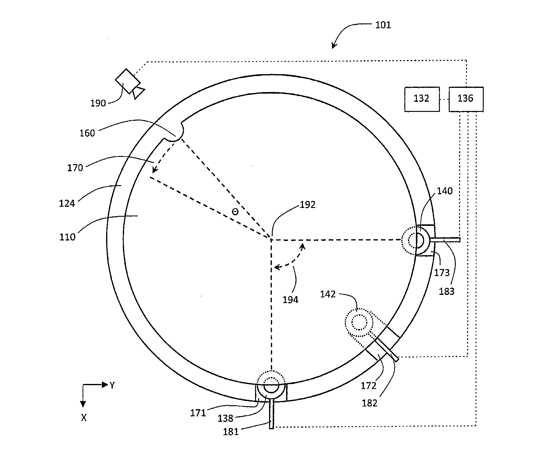
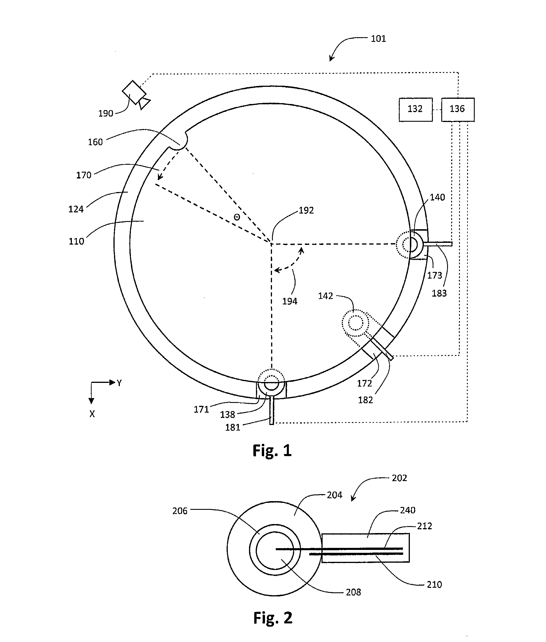
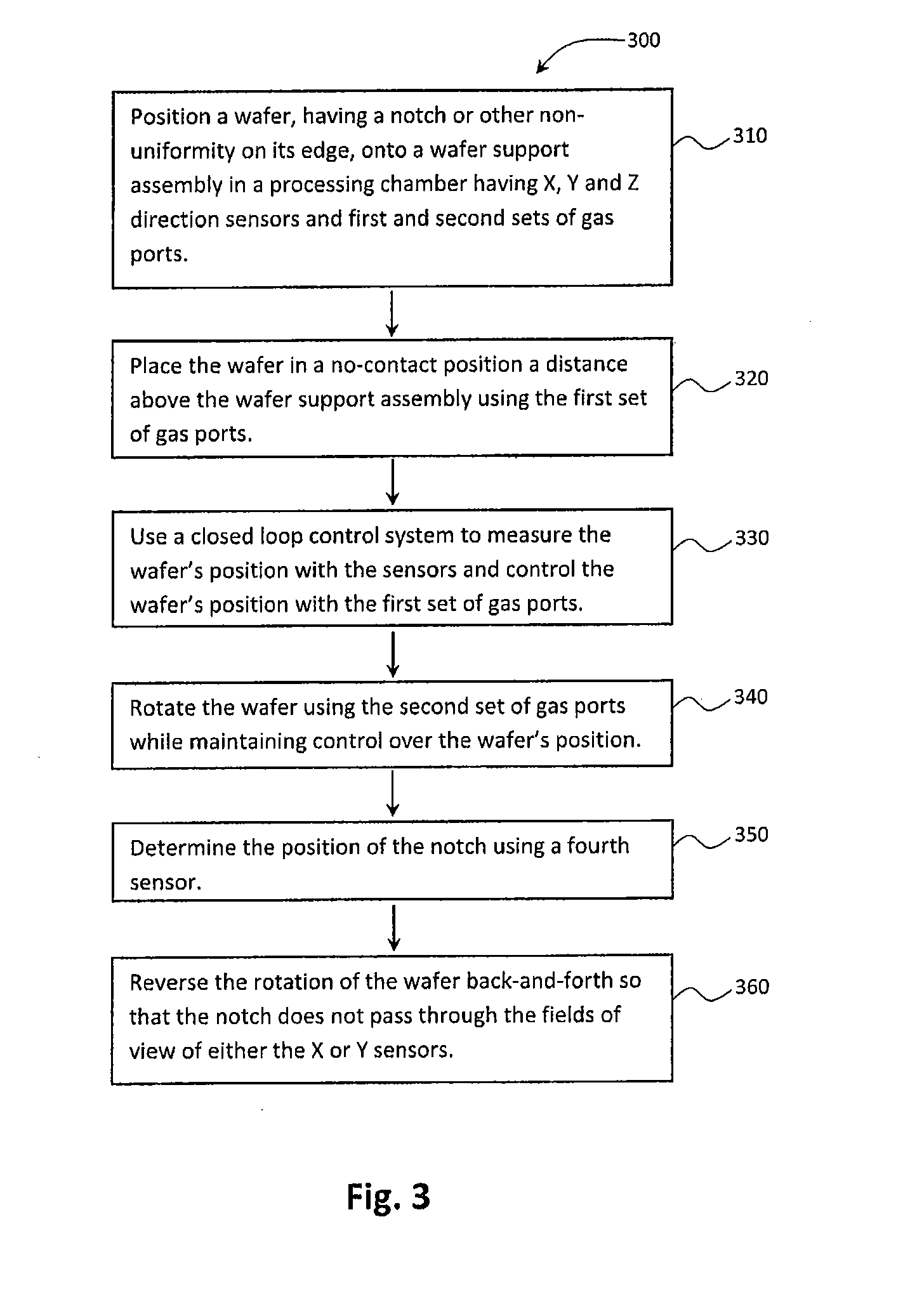
[0029]Embodiments discussed herein provide devices and methods for positioning and / or rotating a substrate, such as a wafer. Further embodiments relate to measuring and controlling position and rotation of a substrate without direct solid contact. (To create a no-contact wafer support system, gas nozzles may be used to float the wafer on a thin layer of gas, air, or other fluids, including liquids. Alternatively, magnetic levitation may be used.) Since there is no solid contact with components of a processing chamber, features on the wafer are used to determine wafer position and rotational speed. Closed loop control systems may be used with sensors to monitor the position of the edge of the wafer in a horizontal plane. Control systems may also monitor the position of a wafer feature as it rotates, such as a notch in the edge of the wafer. Because the presence of a notch can disrupt sensors facing the edge of the wafer, some embodiments provide methods and devices to reduce or elimi...


PUM


Abstract

Devices and methods are provided for positioning and/or rotating a substrate without solid contact, such as by floating the wafer on a thin layer of gas. Since there is no solid contact with components of a processing chamber, features on the wafer are used to determine wafer position and rotational speed. Closed loop control systems are provided with capacitive sensors to monitor the position of the edge of the wafer in a horizontal plane. Control systems may also monitor the position of a wafer feature as it rotates, such as a notch in the edge of the wafer. Because the presence of a notch can disrupt sensors facing the edge of the wafer, methods and devices to reduce or eliminate this disruption are also provided.

Description

CROSS-REFERENCE TO RELATED APPLICATIONS[0001]This application claims benefit of U.S. Provisional Patent Application Ser. No. 61 / 637,984 filed Apr. 25, 2012, which is herein incorporated by reference.BACKGROUND[0002]1. Field[0003]Aspects of the present invention generally relate to methods and devices for positioning and / or rotating a substrate during semiconductor device fabrication in a processing chamber.[0004]2. Description of the Related Art[0005]Integrated circuits are complex devices that can include millions of transistors, capacitors and resistors on a single chip. Chip design continually requires faster circuitry and greater circuit density and thus demands increasingly precise fabrication processes.[0006]In some fabrication processes, such as ion implantation, film layers on the substrate develop high levels of internal stress. In order to relieve the stress and control the film properties and uniformity, the film is subjected to a thermal process, such as annealing. Rapid...

Claims


Application Information

Patent Timeline
IPC IPC(8): H01L21/68
CPCH01L21/681H01L21/67259
Inventor KOELMEL, BLAKE
Owner APPLIED MATERIALS INC
Why Eureka
Try Eureka