Detection device, detection system, and method of manufacturing detection device

Inactive Publication Date: 2013-11-14
CANON KK
View PDF0 Cites 6 Cited by
  • Summary
  • Abstract
  • Description
  • Claims
  • Application Information

AI Technical Summary

Benefits of technology

The present patent provides a detection device that can suppress the decrease in its response characteristics and maintain good response characteristics.

Problems solved by technology

Because the impurity semiconductor layer has much higher specific resistance than the second electrode, an electric field tends to be less efficiently applied to a region of the semiconductor layer, which contacts with the uncovered region of the impurity semiconductor layer, in comparison with the case where the second electrode is disposed over the entire impurity semiconductor layer.
Thus, there is a possibility that response characteristics, e.g., sensitivity and an operation speed, of the detection device may degrade in comparison with those obtained in the case where the second electrode is disposed over the entire impurity semiconductor layer.

Method used


Image

  • Detection device, detection system, and method of manufacturing detection device
  • Detection device, detection system, and method of manufacturing detection device
  • Detection device, detection system, and method of manufacturing detection device

Examples


first embodiment

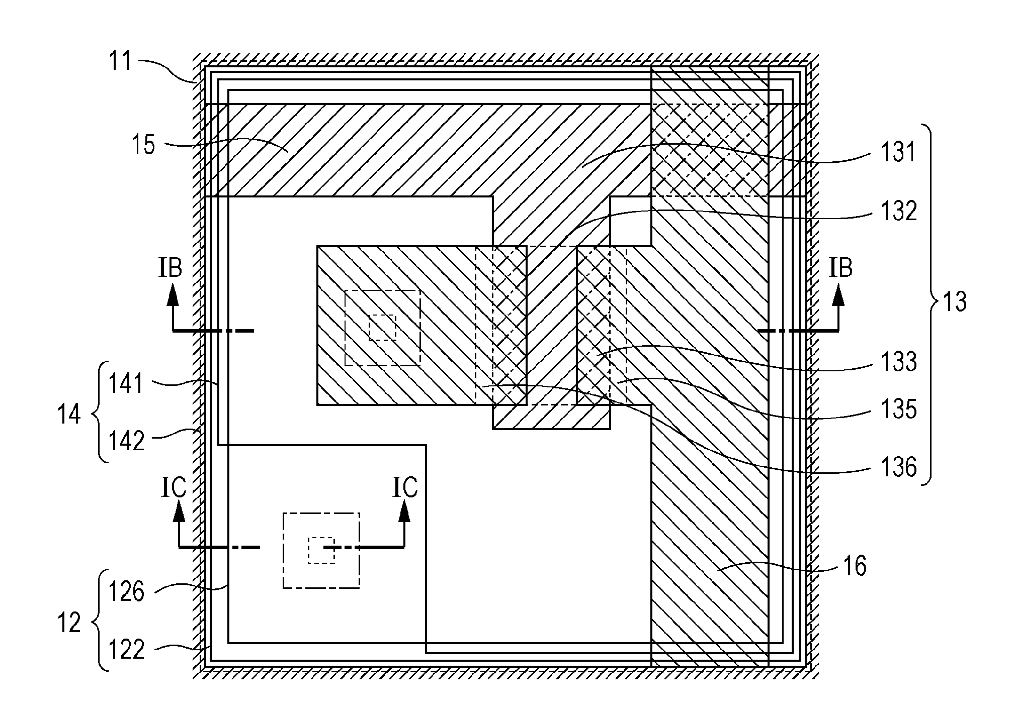
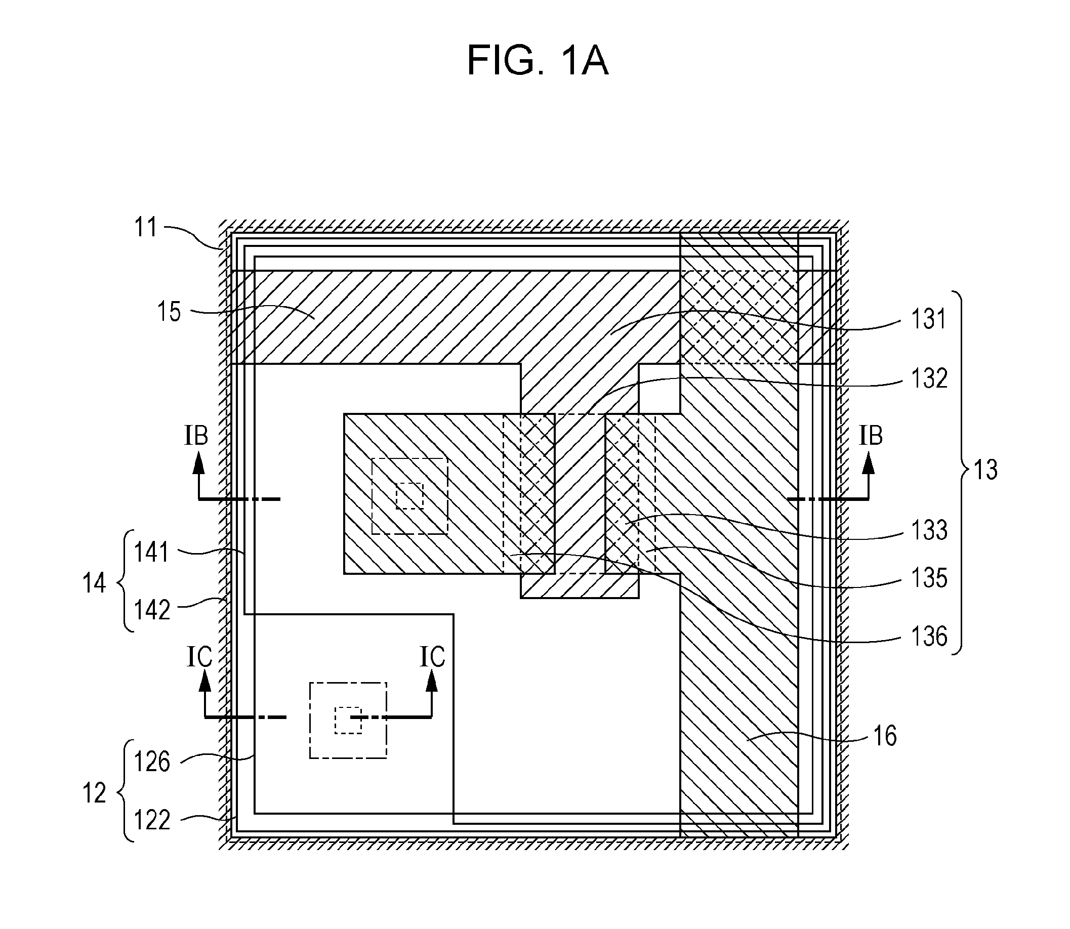
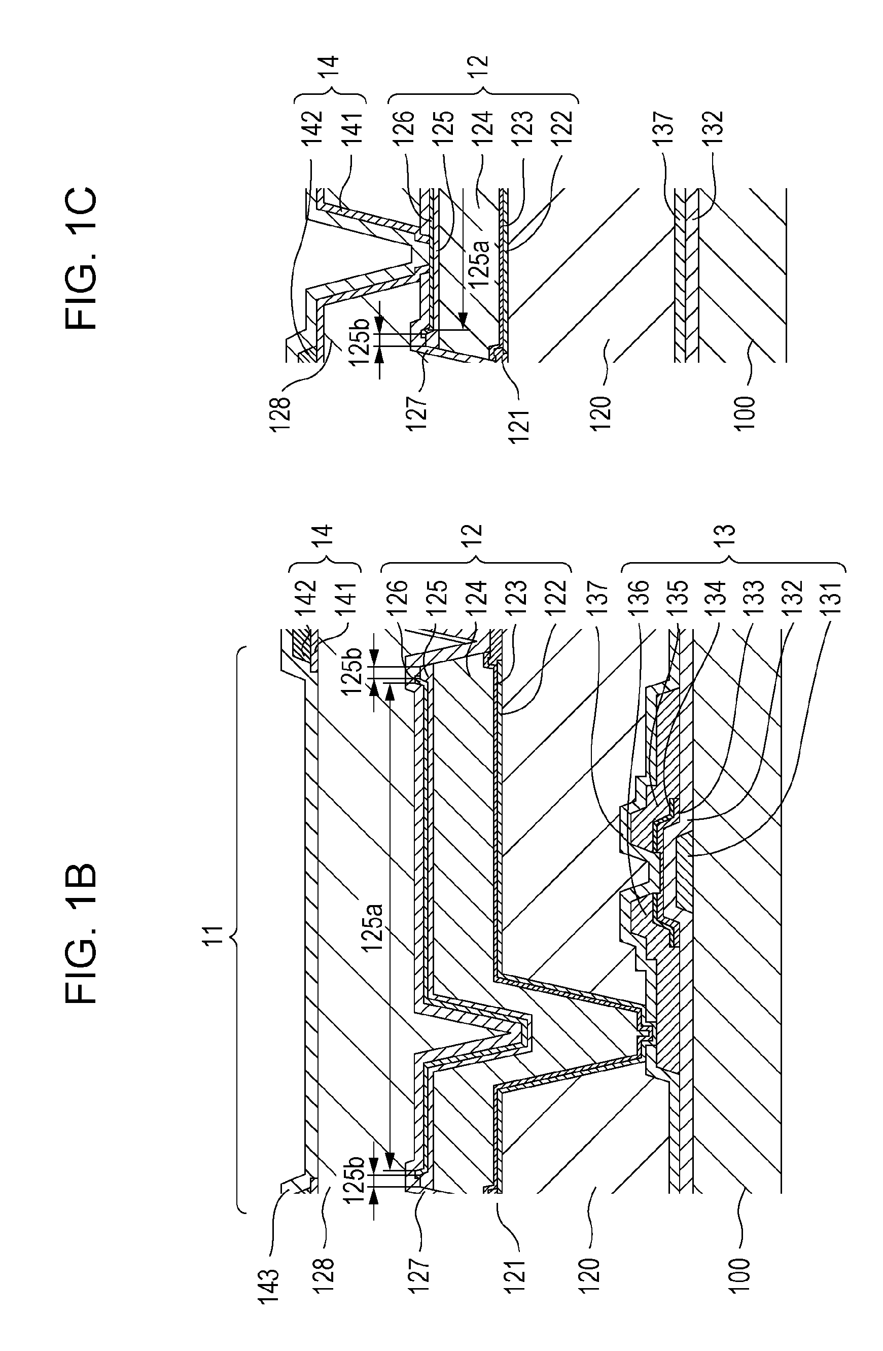
[0027]The structure of one pixel in a detection device according to a first embodiment of the present application is first described with reference to FIG. 1A to 1C. FIG. 1A is a schematic plan view of one of the pixels. In FIG. 1A, insulating layers and a semiconductor layer of a conversion element are omitted for simplification of the drawing. FIG. 1B is a schematic sectional view taken along a line IB-IB in FIG. 1A, and FIG. 1C is a schematic sectional view taken along a line IB-IB in FIG. 1A. The insulating layers and the semiconductor layer of the conversion element, omitted in FIG. 1A, are illustrated in FIGS. 1B and 1C.

[0028]One pixel 11 in the detection device according to the first embodiment of the present disclosure includes a conversion element 12 for converting radiation or light to electric charges, and a TFT (thin-film transistor) 13 serving as a switch element that transfers an electric signal corresponding to the electric charges converted by the conversion element ...

second embodiment

[0051]The structure of one pixel in a detection device according to a second embodiment of the present disclosure will be described below with reference to FIGS. 6A and 6B. FIG. 6A is a schematic sectional view taken along a line corresponding to the line IB-IB in FIG. 1A, and FIG. 6B is a schematic sectional view taken along a line corresponding to the line IC-IC in FIG. 1A.

[0052]In the second embodiment, as illustrated in FIGS. 6A and 6B, a second region 125b of an impurity semiconductor layer is made up of the impurity semiconductor layer 125 called a first impurity semiconductor layer and an impurity semiconductor layer 129 called a second impurity semiconductor layer. In other words, the second region 125b is formed by stacking a plurality of impurity semiconductor layers. With such a structure, the second region 125b of the impurity semiconductor layer has a larger thickness than the first region 125a thereof. The impurity semiconductor layer 129 is an impurity semiconductor l...

third embodiment

[0057]The structure of one pixel in a detection device according to a third embodiment of the present disclosure will be described below with reference to FIGS. 8A and 8B. FIG. 8A is a schematic sectional view taken along a line corresponding to the line IB-IB in FIG. 1A, and FIG. 8B is a schematic sectional view taken along a line corresponding to the line IC-IC in FIG. 1A.

[0058]In the third embodiment, an MIS photoelectric conversion element is used as the conversion element 12 instead of the PIN photodiode in the first embodiment. In more detail, the conversion element 12 includes a first electrode 122, an insulating layer 150, a semiconductor layer 124, an impurity semiconductor layer 151 of first conductivity type, and a second electrode 126, which are successively formed on the first interlayer insulating layer 120 in the mentioned order from the first interlayer insulating layer side. As in the impurity semiconductor layer 125 in the first embodiment, the impurity semiconduct...


PUM


Abstract

A detection device includes conversion elements, each including a first electrode disposed on a substrate, a semiconductor layer disposed on the first electrode, an impurity semiconductor layer disposed on the semiconductor layer and including at least a first region and a second region, and a second electrode disposed on the first region of the impurity semiconductor layer in contact with the impurity semiconductor layer. Sheet resistance in the second region disposed at a position where the impurity semiconductor layer is not contacted with the second electrode is less than sheet resistance in the first region.

Description

BACKGROUND OF THE INVENTION[0001]1. Field of the Invention[0002]The present application relates to a detection device that is applied to, e.g., an image diagnosis apparatus for medical care, a nondestructive inspection apparatus, and an analysis apparatus using radiation. The present application further relates to a detection system and a method of manufacturing the detection device.[0003]2. Description of the Related Art[0004]Recently, the thin-film semiconductor manufacturing technology has been employed to manufacture a detection device including an array of pixels (pixel array), which is a combination of switch elements, e.g., thin-film transistors (TFTs), and conversion elements, e.g., photodiodes, for converting radiation or light to electric charges.[0005]Each of pixels in related-art detection devices disclosed in Japanese Patent Laid-Open No. 2004-296654 and No. 2007-059887 includes a conversion element including a first electrode disposed on a substrate, a second electrode...

Claims


Application Information

Patent Timeline
IPC IPC(8): H01L27/146G01T1/24
CPCH01L27/14643H01L27/14683G01T1/24H01L27/14632H01L27/14676H01L27/14687
Inventor MOCHIZUKI, CHIORIWATANABE, MINORUYOKOYAMA, KEIGOOFUJI, MASATOKAWANABE, JUNFUJIYOSHI, KENTAROWAYAMA, HIROSHI
Owner CANON KK
Why Eureka
Try Eureka