Spin Transistors Employing a Piezoelectric Layer and Related Memory, Memory Systems, and Methods

a piezoelectric layer and piezoelectric technology, applied in the manufacture/treatment of galvano-magnetic devices, semiconductor devices, electrical apparatus, etc., can solve the problems of low power alternatives, power consumption in charge based switches, and conventional mtjs consuming certain amounts of power in switching between states

Active Publication Date: 2013-11-14
QUALCOMM INC
View PDF2 Cites 14 Cited by
  • Summary
  • Abstract
  • Description
  • Claims
  • Application Information

AI Technical Summary

Benefits of technology

[0012]Embodiments disclosed in the detailed description include spin transistors and related memory, memory systems, and methods. A spin transistor is provided by at least two magnetic tunnel junctions (MTJs) with a shared multiferroic layer. In one embodiment, the multiferroic layer is formed from a piezoelectric (PE) thin film over a ferromagnetic thin film (FM channel) with a metal electrode (metal). The ferromagnetic layer functions as the spin channel and the piezoelectric layer is used for transferring piezoelectric stress to control the spin state of the channel. The MTJ on one side of the shared layer forms a source and the MTJ on the other side is a drain for the spin transistor. When a voltage pulse is provided to the PE film, the PE film induces stress against the ferromagnetic layer. The induced stress-anisotropy in the ferromagnetic layer in turn leads to a ninety degree rotation of the favorable spin orientation (easy axis) from an initially Parallel or Anti-parallel state. This rotation sets up a meta-stable spin state. When a small voltage between a source and drain of the spin transistor is applied, a small spin polarized current collapses the spin state to a parallel orientation and turns the channel to a low impedance state, completing the spin transistor on-state transition. When there is no voltage between the source and drain, the magnetic dipole forces the spin state to Anti-parallel and changes the channel to a high impedance state, completing the off-state transition.

Problems solved by technology

Power consumption in such charge based switches remains a concern and there remains continued pressure to find low power alternatives to existing switching technology.
However, conventional MTJs consume certain amounts of power in switching between states.
Power consumption shortens battery life in mobile terminals such as mobile phones and generates waste heat which must be dissipated in all devices.

Method used


Image

  • Spin Transistors Employing a Piezoelectric Layer and Related Memory, Memory Systems, and Methods
  • Spin Transistors Employing a Piezoelectric Layer and Related Memory, Memory Systems, and Methods
  • Spin Transistors Employing a Piezoelectric Layer and Related Memory, Memory Systems, and Methods

Examples


Embodiment Construction

[0028]With reference now to the drawing figures, several exemplary embodiments of the present disclosure are described. The word “exemplary” is used herein to mean “serving as an example, instance, or illustration.” Any embodiment described herein as “exemplary” is not necessarily to be construed as preferred or advantageous over other embodiments.

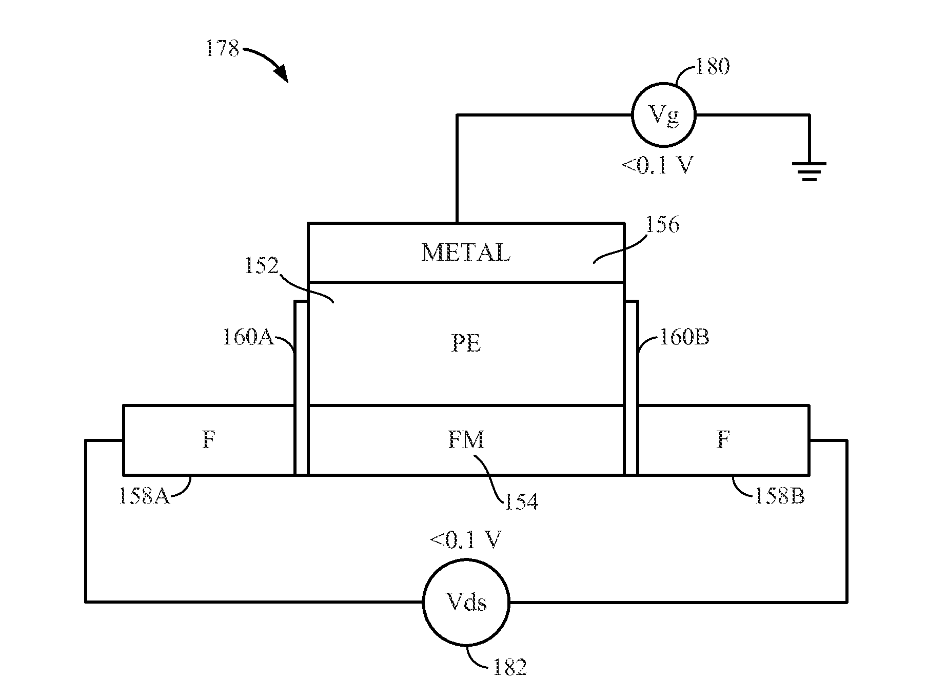
[0029]Embodiments disclosed in the detailed description include spin transistors and related memory, memory systems, and methods. A spin transistor is provided by at least two magnetic tunnel junctions (MTJs) with a shared multiferroic layer. In one embodiment, the multiferroic layer is formed from a piezoelectric (PE) thin film over a ferromagnetic thin film (FM channel) with a metal electrode (metal). The ferromagnetic layer functions as the spin channel and the piezoelectric layer is used for transferring piezoelectric stress to control the spin state of the channel. The MTJ on one side of the shared layer forms a source and the MTJ on ...


PUM


Abstract

Spin transistors and related memory, memory systems, and methods are disclosed. A spin transistor is provided by at least two magnetic tunnel junctions (MTJs) with a shared multiferroic layer. The multiferroic layer is formed from a piezoelectric (PE) thin film over a ferromagnetic thin film (FM channel) with a metal electrode (metal). The ferromagnetic layer functions as the spin channel and the piezoelectric layer is used for transferring piezoelectric stress to control the spin state of the channel. The MTJ on one side of the shared layer forms a source and the MTJ on the other side is a drain for the spin transistor.

Description

PRIORITY CLAIM[0001]The present application claims priority to and the benefit of U.S. Patent Application Ser. No. 61 / 644,592 filed on 9 May 2012 and entitled “SPIN TRANSISTORS AND RELATED MEMORY, MEMORY SYSTEMS, AND METHODS,” which is incorporated herein by reference in its entirety.BACKGROUND[0002]I. Field of the Disclosure[0003]The technology of the disclosure relates generally to magnetic tunnel junctions (MTJs) used to provide memory cells.[0004]II. Background[0005]The electronics industry commonly uses switches as a component of circuit design. To date, these switches have been charge based switches, such as a CMOS or MOSFET switch. Power consumption in such charge based switches remains a concern and there remains continued pressure to find low power alternatives to existing switching technology.[0006]Magnetic tunnel junctions (MTJs) can be used as switches, but are more frequently used in memory applications, such as magnetic random access memory (MRAM), which is non-volatil...

Claims


Application Information

Patent Timeline
Patent Type & Authority Applications(United States)
IPC IPC(8): H01L43/02H01L43/12
CPCH01L43/02H01L43/12H01L29/66984H10N50/10H10N50/01H10B61/22H10N50/80
Inventor DU, YANG
Owner QUALCOMM INC
Why Eureka
Try Eureka