Semiconductor memory device and method of operating the same

a memory device and semiconductor technology, applied in the field of semiconductor memory devices, can solve the problems of affecting the operation of the memory cell, the threshold voltage of the memory cell to change, and the process of three-dimensional structures is unstable, so as to reduce the number of times a pass voltage is applied, and reduce the disturbance based on the pass voltage

Active Publication Date: 2013-11-14
SK HYNIX INC
View PDF2 Cites 6 Cited by
  • Summary
  • Abstract
  • Description
  • Claims
  • Application Information

AI Technical Summary

Benefits of technology

[0010]A semiconductor memory device and a method of operating the same according to the present invention minimizes the number of times a pass voltage is applied to a non-selected memory cell when a program operation is performed, thus reducing the disturbance based on the pass voltage.

Problems solved by technology

However, a problem exists in that a process for three-dimensional structures is unstable and / or the reliability of the memory device has deteriorated in the new three-dimensional structure.
Accordingly, a problem exists in that the number of times a pass voltage is applied to each word line increases every time a program operation is performed, causing the threshold voltage of the memory cell to change based on the pass voltage.

Method used


Image

  • Semiconductor memory device and method of operating the same
  • Semiconductor memory device and method of operating the same
  • Semiconductor memory device and method of operating the same

Examples


Embodiment Construction

[0019]Hereinafter, the preferred embodiments of the present invention will be explained in more detail with reference to the accompanying drawings. Although embodiments have been described with reference to a number of illustrative embodiments thereof, it should be understood that numerous other modifications and embodiments can be devised by those skilled in the art that will fall within the spirit and scope of the principles of this disclosure.

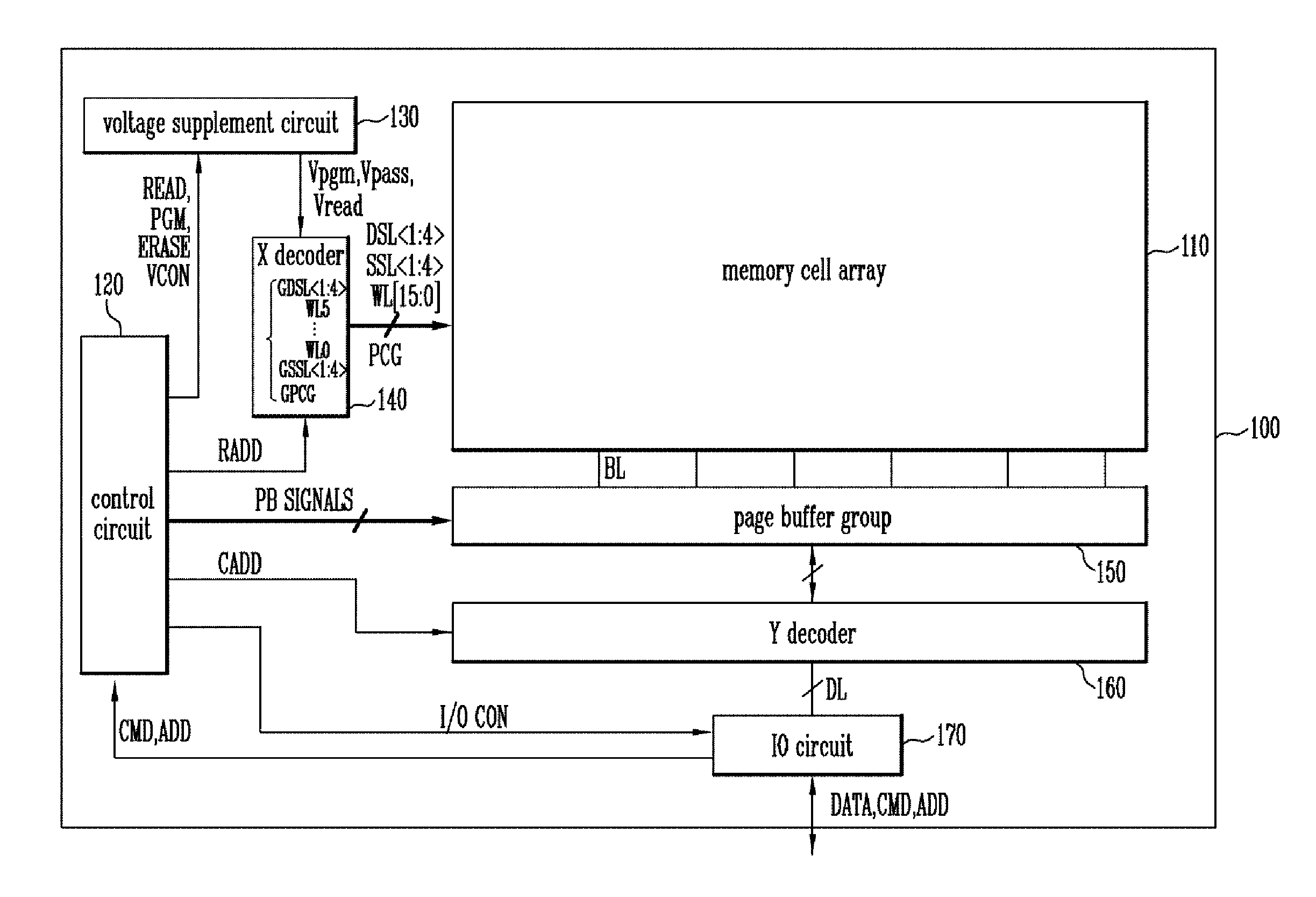
[0020]FIG. 1 is a view illustrating a semiconductor memory device according to an embodiment of the present invention.

[0021]In FIG. 1, a semiconductor memory device 100 includes a memory cell array 110 having memory cells.

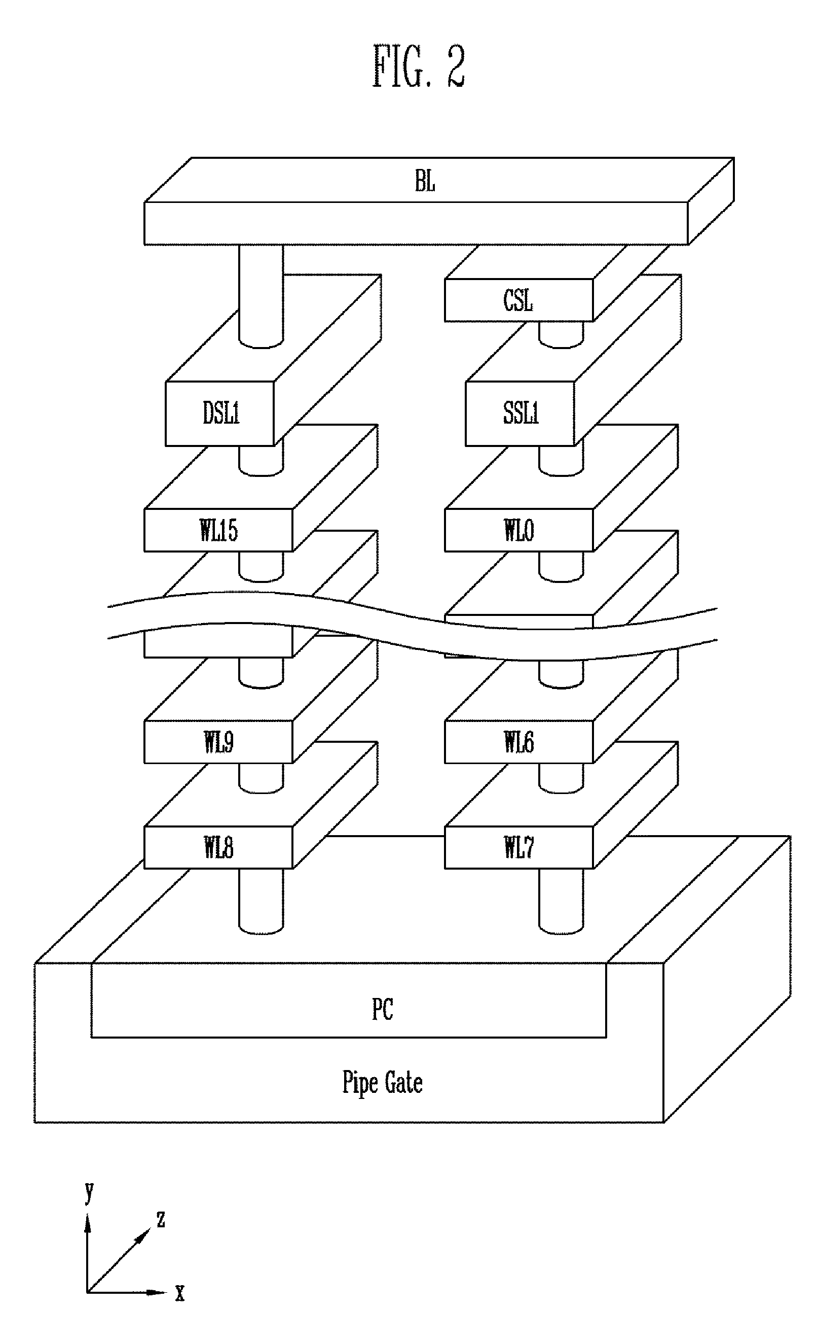
[0022]The memory cell array 110 has three-dimensional structure, and the structure will be described in detail below.

[0023]The semiconductor memory device 100 includes a peripheral circuit group 130 to 170 that serves to program the memory cells or read data stored in the memory cell, and a control circuit 120 that serves t...


PUM


Abstract

A semiconductor memory device of the present invention includes a memory cell array with cell strings having word lines stacked on a substrate and a vertical channel layer formed through the word lines, a peripheral circuit configured to select one of the word lines and perform a program operation on the selected word line, and a control circuit configured to control the peripheral circuit to perform the program operation by applying a program voltage to a word line selected for the program operation, applying a ground voltage to a word line of which a program operation has been completed and applying a pass voltage to the other word lines.

Description

CROSS-REFERENCE TO RELATED APPLICATION[0001]This application claims priority from Korean Patent Application No. 10-2012-0048770, filed on May 8, 2012, the contents of which are incorporated herein by reference in its entirety.BACKGROUND[0002]The present invention relates generally to a semiconductor memory device and a method of operating the same.[0003]High density memory has been continuously required since manufacturing techniques for semiconductors have improved. A memory device having three-dimensional structure, where memory cells are vertically stacked on a silicon substrate, has been suggested, since a memory device having two-dimensional structure, where the memory cells are formed with one layer on the silicon substrate is reaching a limit.[0004]However, a problem exists in that a process for three-dimensional structures is unstable and / or the reliability of the memory device has deteriorated in the new three-dimensional structure. Various methods for solving the problem h...

Claims


Application Information

Patent Timeline
Patent Type & Authority Applications(United States)
IPC IPC(8): G11C7/00
CPCG11C7/02G11C8/08G11C8/14G11C16/10G11C16/08
Inventor HUH, HWANG
Owner SK HYNIX INC
Why Eureka
Try Eureka