Touch display panel

a display panel and touch technology, applied in the direction of thermoelectric device junction materials, electrical apparatus, semiconductor devices, etc., can solve the problems of reducing the transmittance, reducing the thickness of the conventional touch display device, and reducing the transmittance, so as to achieve the effect of increasing the thickness

Inactive Publication Date: 2013-11-21
WINTEK CORP
View PDF3 Cites 25 Cited by
  • Summary
  • Abstract
  • Description
  • Claims
  • Application Information

AI Technical Summary

Benefits of technology

[0006]The present invention provides a touch display panel which uses an organic light emitting diode structure to display, wherein the first electrode layer of the organic light emitting diode structure includes the touch sensing electrodes. Thus, the touch display panel can have the functions of touch sensing and displaying without needing to greatly increase the thickness.

Problems solved by technology

Therefore, the conventional touch display device is comparatively thicker and heavy.
In addition, the design of externally assembling the touch panel to the display panel may easily cause the degradation of transmittance.

Method used


Image

  • Touch display panel
  • Touch display panel
  • Touch display panel

Examples


Embodiment Construction

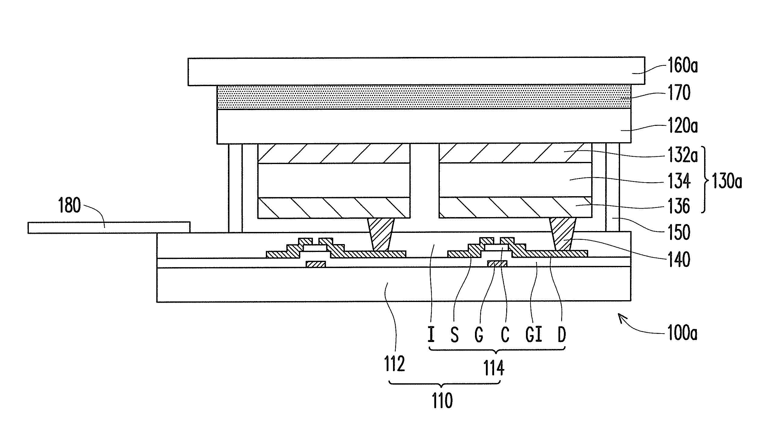
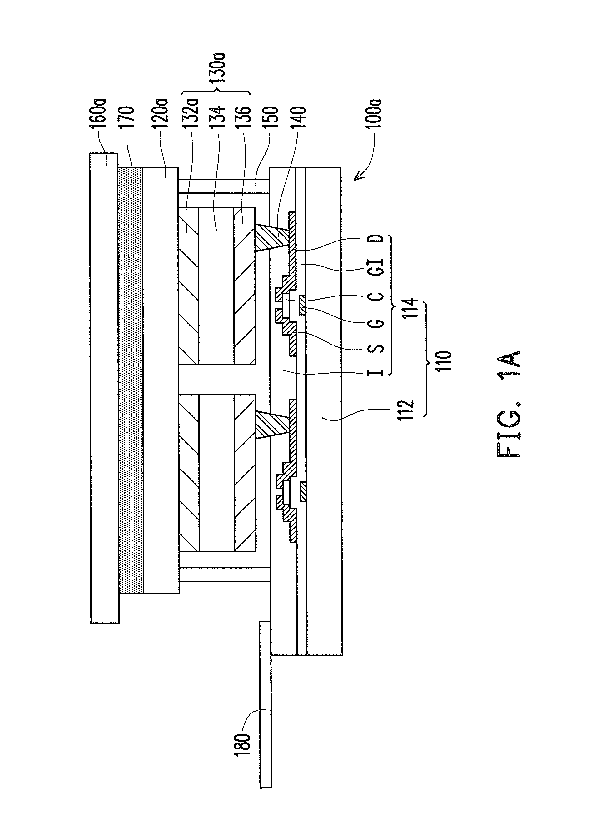
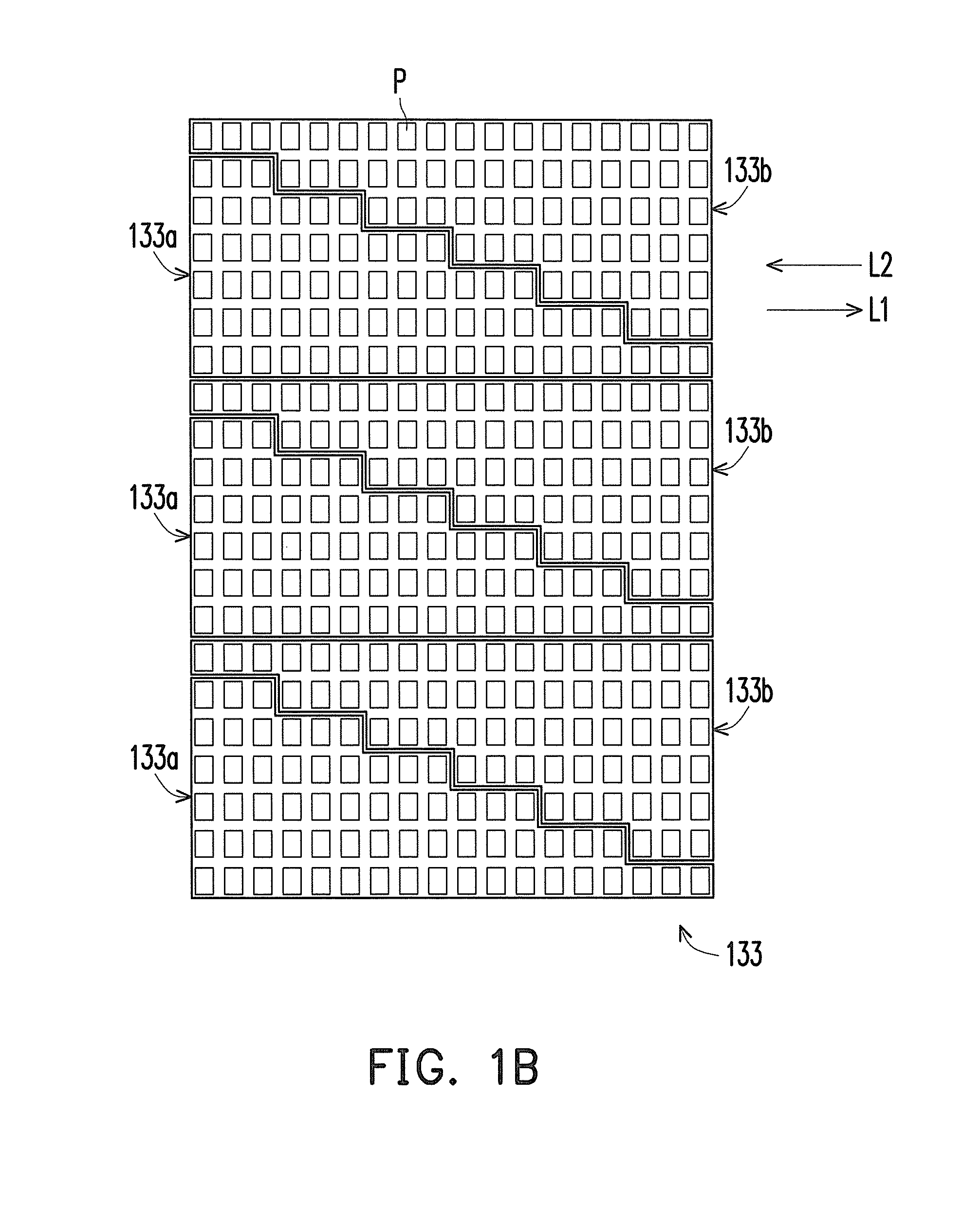
[0027]FIG. 1A schematically shows a cross-sectional view of a touch display panel according to an exemplary embodiment of the present invention. FIG. 1B illustrates a top view of the touch sensing electrodes in FIG. 1A. Referring to FIG. 1A, in the embodiment, the touch display panel 100a includes an array substrate 110, an opposite substrate 120a, an organic light emitting structure 130a, a plurality of conductive spacers 140 and a sealant 150.

[0028]In more detailed, the array substrate 110 is an active device array substrate including a substrate 112 and a plurality of active devices 114. Each of the active devices 114 includes a gate G, a gate insulating layer GI, a channel layer C, a source S, a drain D and an insulating layer I, for example. Herein the gate G is located on the substrate 112, and the gate insulating layer GI, the channel layer C, the source S / drain D and the insulating layer I are sequentially stacked on the substrate 112. In other embodiments not shown in the f...


PUM


Abstract

A touch display panel including a array substrate, an opposite substrate, an organic light emitting diode (OLED) structure, a plurality of conductive spacers and a sealant is provided. The OLED structure is disposed on the opposite substrate and located between the array substrate and the opposite substrate. The OLED structure includes a first electrode layer, an organic light emitting layer and a second electrode layer which are sequentially disposed. The first electrode layer is located on the opposite substrate and includes a plurality of touch sensing electrode. The second electrode layer is electrically connected to the array substrate via the conductive spacers. The sealant is sealed the OLED structure and the conductive spacers between the array substrate and the opposite substrate.

Description

CROSS-REFERENCE TO RELATED APPLICATION[0001]This application claims the priority benefit of Taiwan application serial no. 101117246, filed on May 15, 2012. The entirety of the above-mentioned patent application is hereby incorporated by reference herein and made a part of this specification.BACKGROUND OF THE INVENTION[0002]1. Field of the Invention[0003]The present invention generally relates to a touch display panel, and more particularly, to a touch display panel in which organic light emitting layer is used to display.[0004]2. Description of Related Art[0005]In general, a conventional touch display device is a display panel externally assembled with an independent touch panel. Therefore, the conventional touch display device is comparatively thicker and heavy. In addition, the design of externally assembling the touch panel to the display panel may easily cause the degradation of transmittance. Thus, if the touch sensing function can be directly integrated in a display device, th...

Claims


Application Information

Patent Timeline
Patent Type & Authority Applications(United States)
IPC IPC(8): H01L27/32
CPCH01L27/323H10K59/40H10K59/127
Inventor CHANG, TING-YUHSU, CHING-FUWU, YU-HUACHANG, YU-CHENGWANG, WEN-CHUN
Owner WINTEK CORP
Why Eureka
Try Eureka