Electronic device comprising rf-ldmos transistor having improved ruggedness
a technology of rfldmos and ruggedness, which is applied in the direction of limiting amplitude using diodes, diodes, semiconductor devices, etc., can solve the problem of low power dissipation of rectifying elements, and achieve the effect of improving rf ruggedness and compromising the rf performance of rfldmos
- Summary
- Abstract
- Description
- Claims
- Application Information
AI Technical Summary
Benefits of technology
Problems solved by technology
Method used
Image
Examples
first embodiment
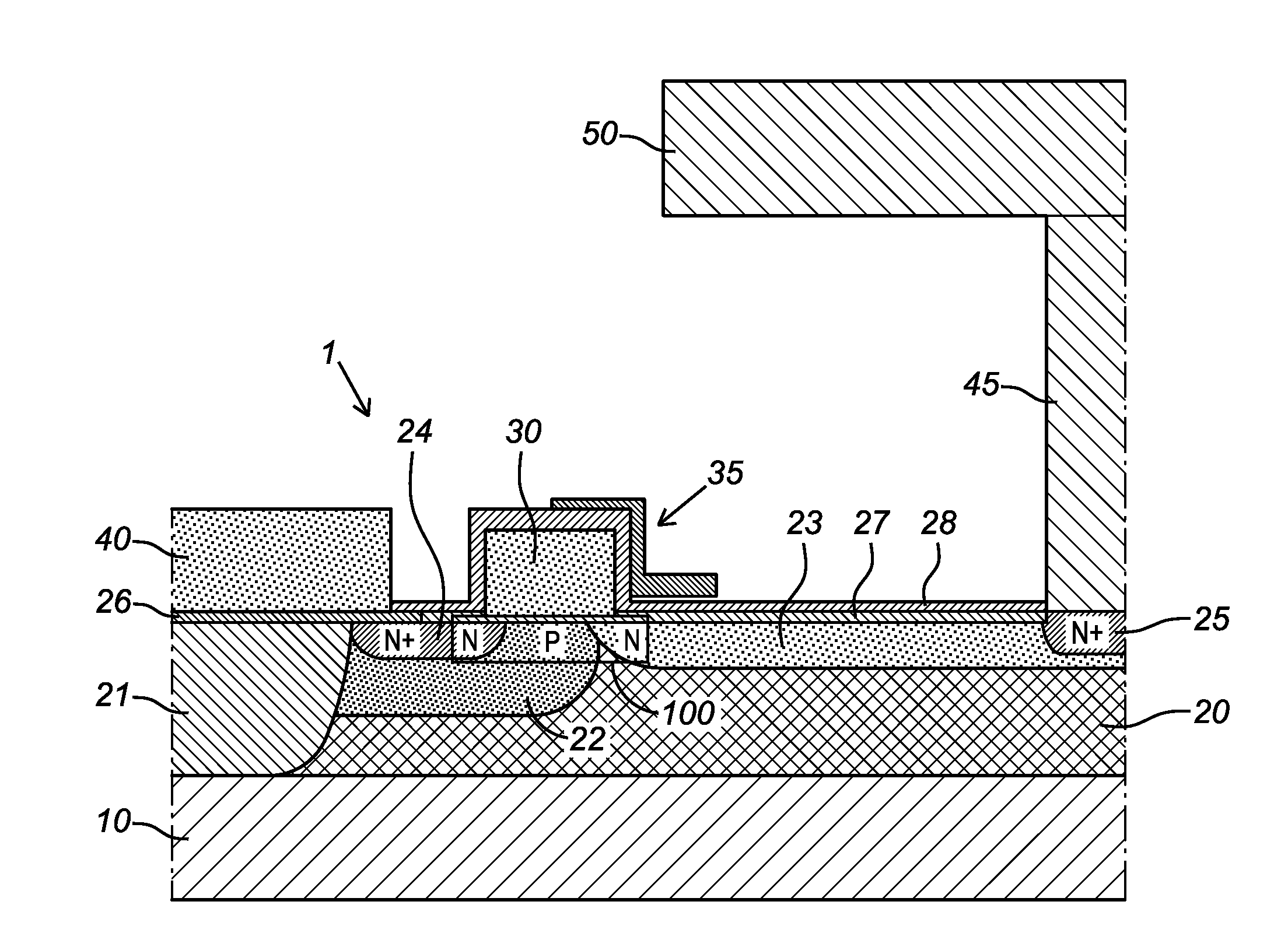
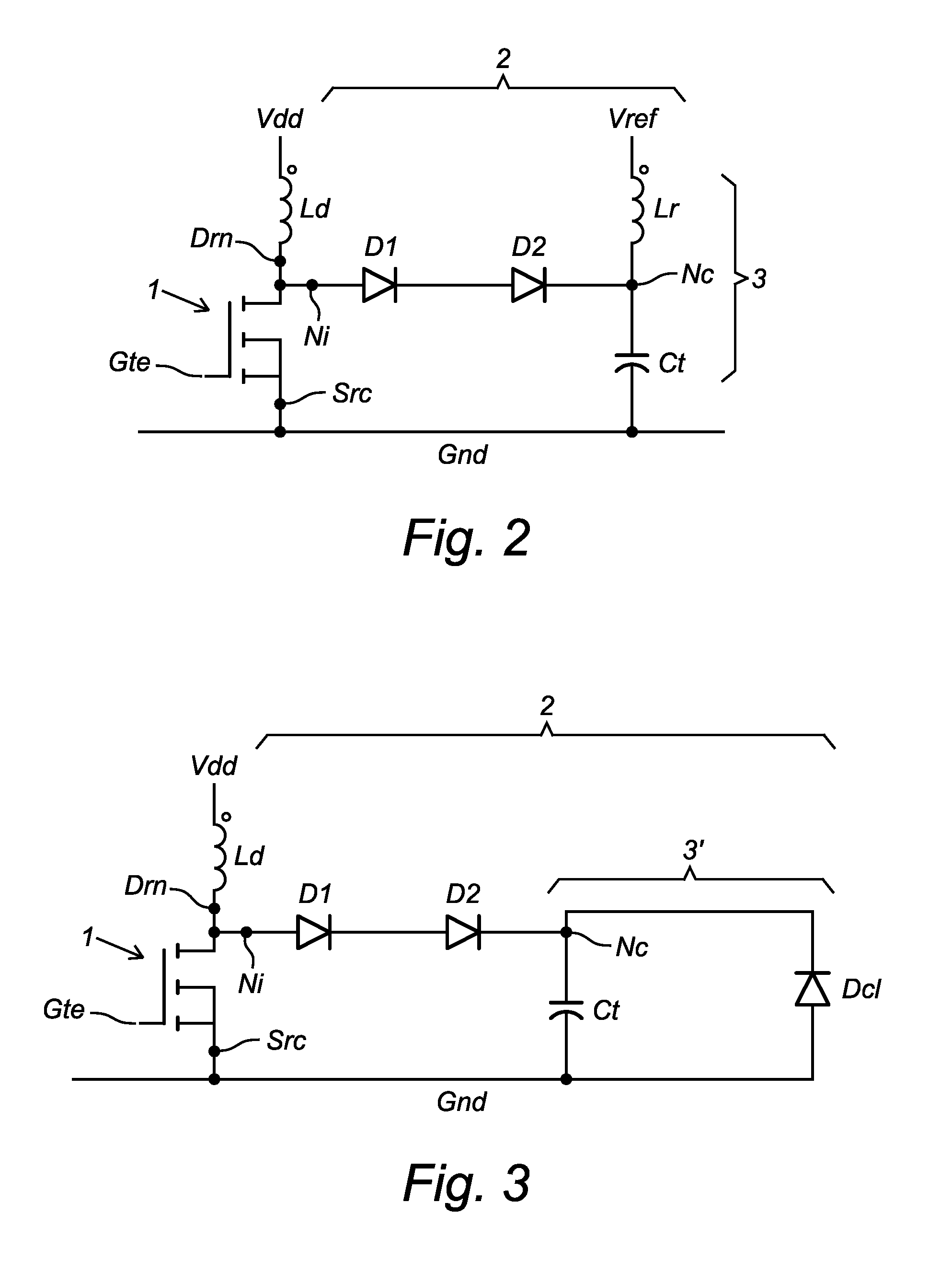
[0101]FIG. 2 shows an equivalent circuit diagram of an electronic device in accordance with the invention. On the left side of FIG. 2 there is shown the RF-LDMOS transistor 1 which is connected, via a drain terminal bondwire Ld (with an inductance), with its drain terminal Drn to a drain lead connected to a power supply voltage Vdd. This supply voltage Vdd is typically within the range of 28V to 50V. An LDMOS device optimized for 28V will have slightly other dimensions then the 50V variant. The RF-LDMOS transistor also comprises a gate terminal Gte which is typically connected to a gate lead via a further bondwire (not shown). The source terminal Src of the LDMOS transistor 1 is connected to the ground voltage (potential) Gnd. As already mentioned the source terminal of the RF-LDMOS is typically at the backside of a substrate. Typically, the substrate onto which the RF-LDMOS is manufactured is directly provided on and in electrical contact with a source lead.
[0102]The electronic dev...
second embodiment
[0108]FIG. 3 shows an equivalent circuit diagram of an electronic device in accordance with the invention. This embodiment will be discussed in as far as it differs from FIG. 2. Sometimes, it may be inconvenient to feed the extra reference voltage Vref via additional bondwires to the chip. In the embodiment of FIG. 3 the reference voltage is created on the die itself. The main difference between FIG. 3 and FIG. 2 is that in FIG. 3 there is an alternative clipping circuit 3′. The alternative clipping circuit 3′ comprises the capacitance Ct and a clipping diode Dcl connected in parallel with the capacitance Ct, wherein the anode side of the clipping diode Dcl is connected to the ground voltage (further reference voltage terminal), i.e. in normal operation the clipping diode Dcl is reverse-biased.
[0109]A clipping diode Dcl with a breakdown voltage equal to the earlier mentioned reference voltage Vref in FIG. 2, is integrated near to capacitance Ct. This clipping diode Dcl must be able ...
PUM
 Abstract
Description
Claims
Application Information


