Composite writer shield for improving writer performance
a writer and shield technology, applied in the field of composite shields, can solve the problems of reducing limiting the reader spacing, so as to improve the writing current saturation speed, improve the writing speed, and improve the writing speed
- Summary
- Abstract
- Description
- Claims
- Application Information
AI Technical Summary
Benefits of technology
Problems solved by technology
Method used
Image
Examples
second embodiment
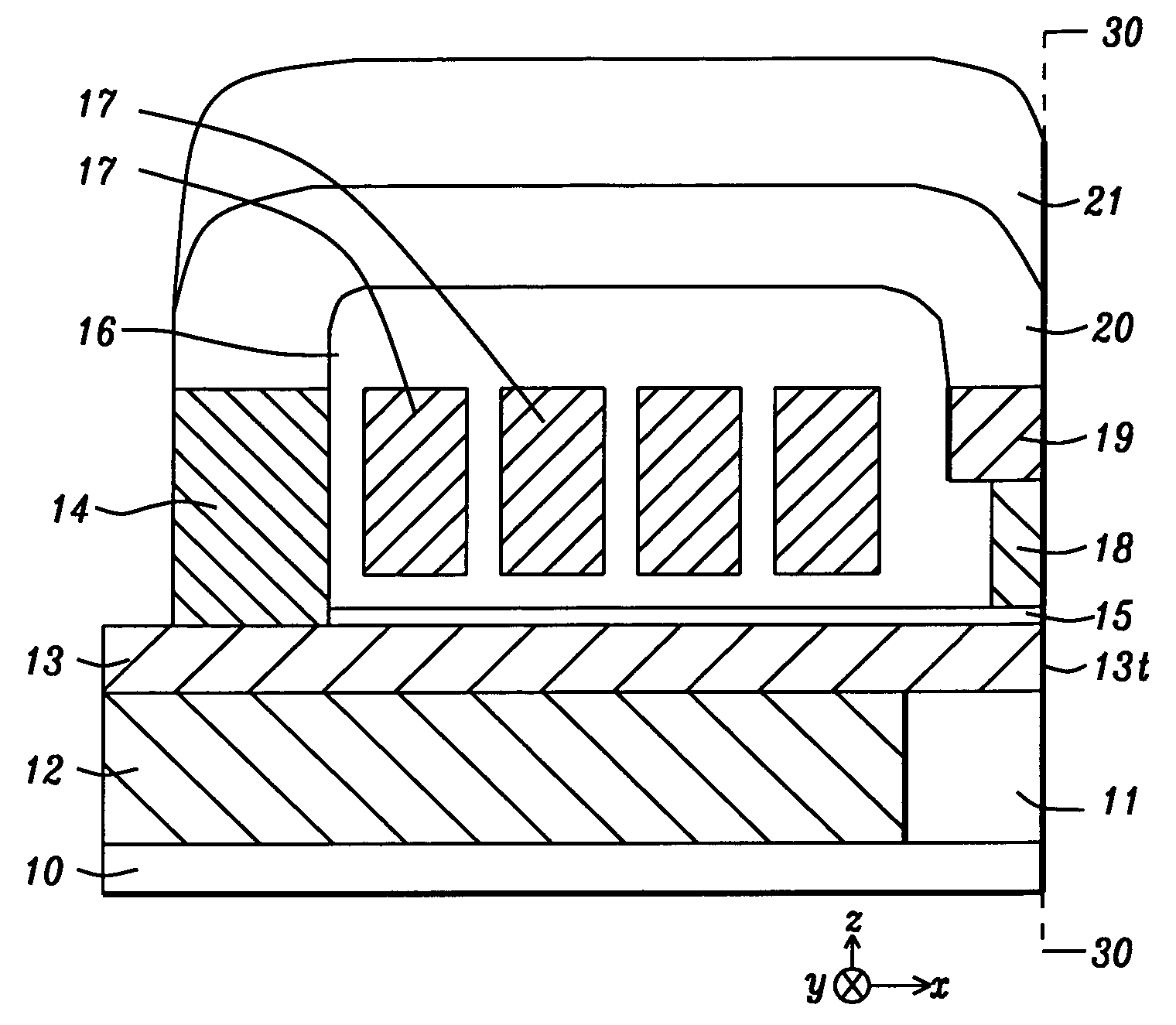
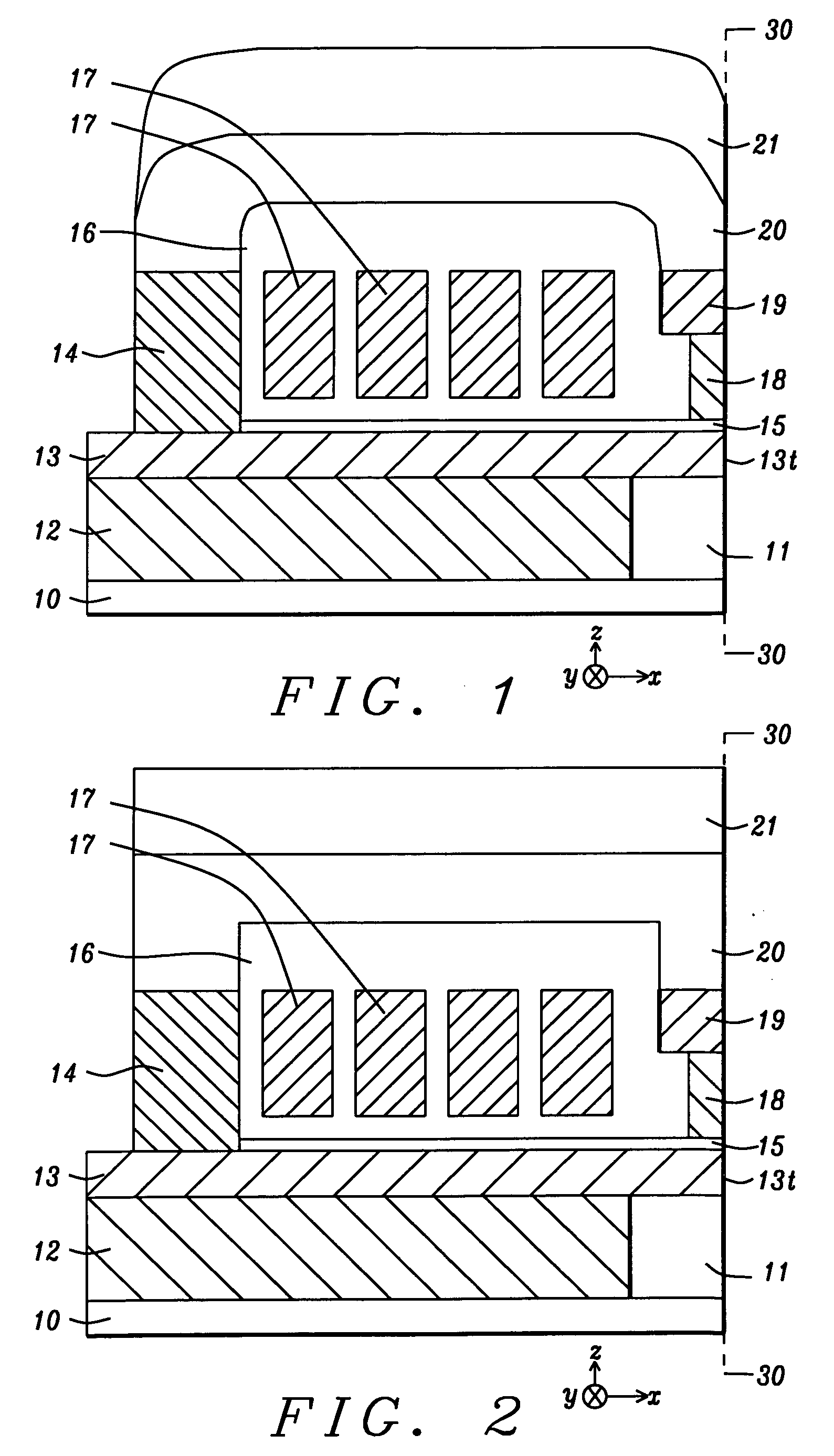
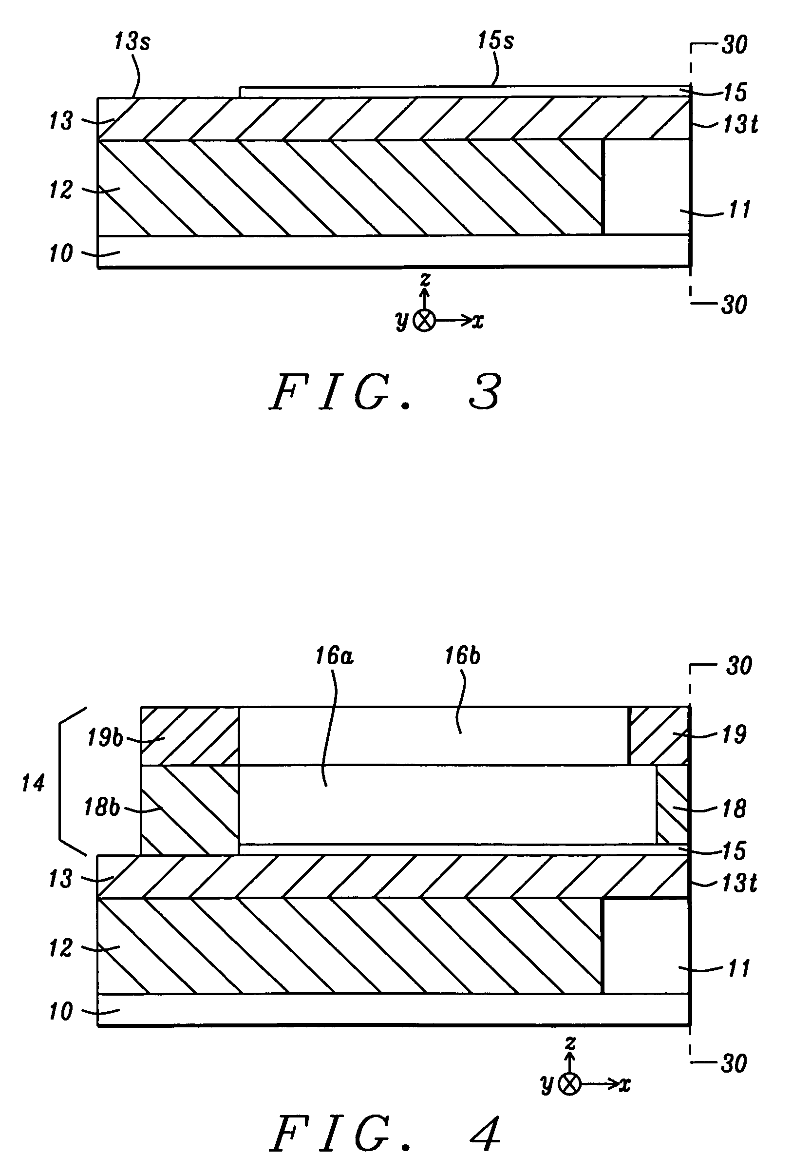
[0027]First a method of forming the PMR writer according to the present invention will be described. Referring to FIG. 3, a cross-sectional view is shown from a plane that is perpendicular to an air bearing surface (ABS) 30-30. There is a substrate 10 that may be a separation layer made of Al2O3 between a read head (not shown) and the PMR write head as described herein and shown in its entirety in FIGS. 1-2. The embodiment illustrated in FIG. 1 includes an arched shape for the upper shield section comprised of a lower layer 20, and upper layer 21 where lower layer is defined as the layer that connects with a second write shield and is closer to the main pole layer 13. A second embodiment in FIG. 2 shows an upper shield section with lower layer 20, and upper layer 21 that have essentially planar top surfaces opposite the main pole layer 13. It should be understood that the substrate 10 may be part of a slider (not shown) formed in an array of sliders on a wafer. After the PMR write h...
first embodiment
[0028]Returning to FIG. 3, a first embodiment is depicted wherein an etch stop layer (not shown) such as Ru may be deposited on the substrate 10. A first insulation layer 11 is deposited on the etch stop layer by a physical vapor deposition (PVD) or chemical vapor deposition (CVD) method. An opening (not shown) corresponding to the shape of the bottom yoke is formed in the first insulation layer 11 by conventional photoresist patterning and etching steps. After the patterned photoresist layer is stripped, a seed layer (not shown) may be deposited in the opening. Thereafter, the bottom yoke 12 may be formed by an electroplating method and is made coplanar with the first insulation layer by a chemical mechanical polish (CMP) step. The main pole layer 13 including pole tip 13t at the ABS 30-30 may be formed in a similar fashion by depositing a second insulation layer (not shown) on the first insulation layer 11 and bottom yoke 12 followed by forming an opening in the second insulation ...
PUM
| Property | Measurement | Unit |
|---|---|---|
| thickness | aaaaa | aaaaa |
| thickness | aaaaa | aaaaa |
| thickness | aaaaa | aaaaa |
Abstract
Description
Claims
Application Information


