

Method for manufacturing transistor
- Summary
- Abstract
- Description
- Claims
- Application Information
AI Technical Summary
Benefits of technology
Problems solved by technology
Method used
Image

Examples
Embodiment Construction
[0029]Hereinafter, the present invention will be described in detail by means of embodiments thereof and with reference to the drawings.
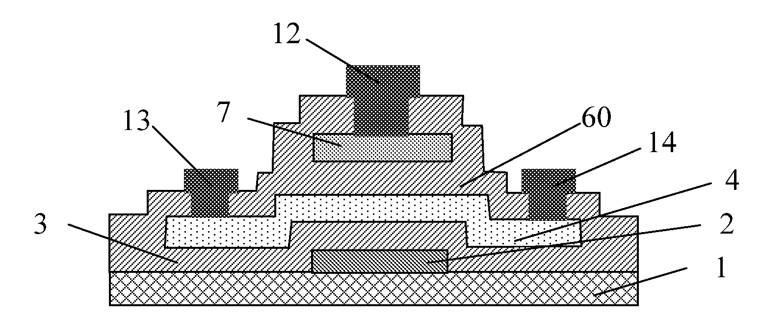
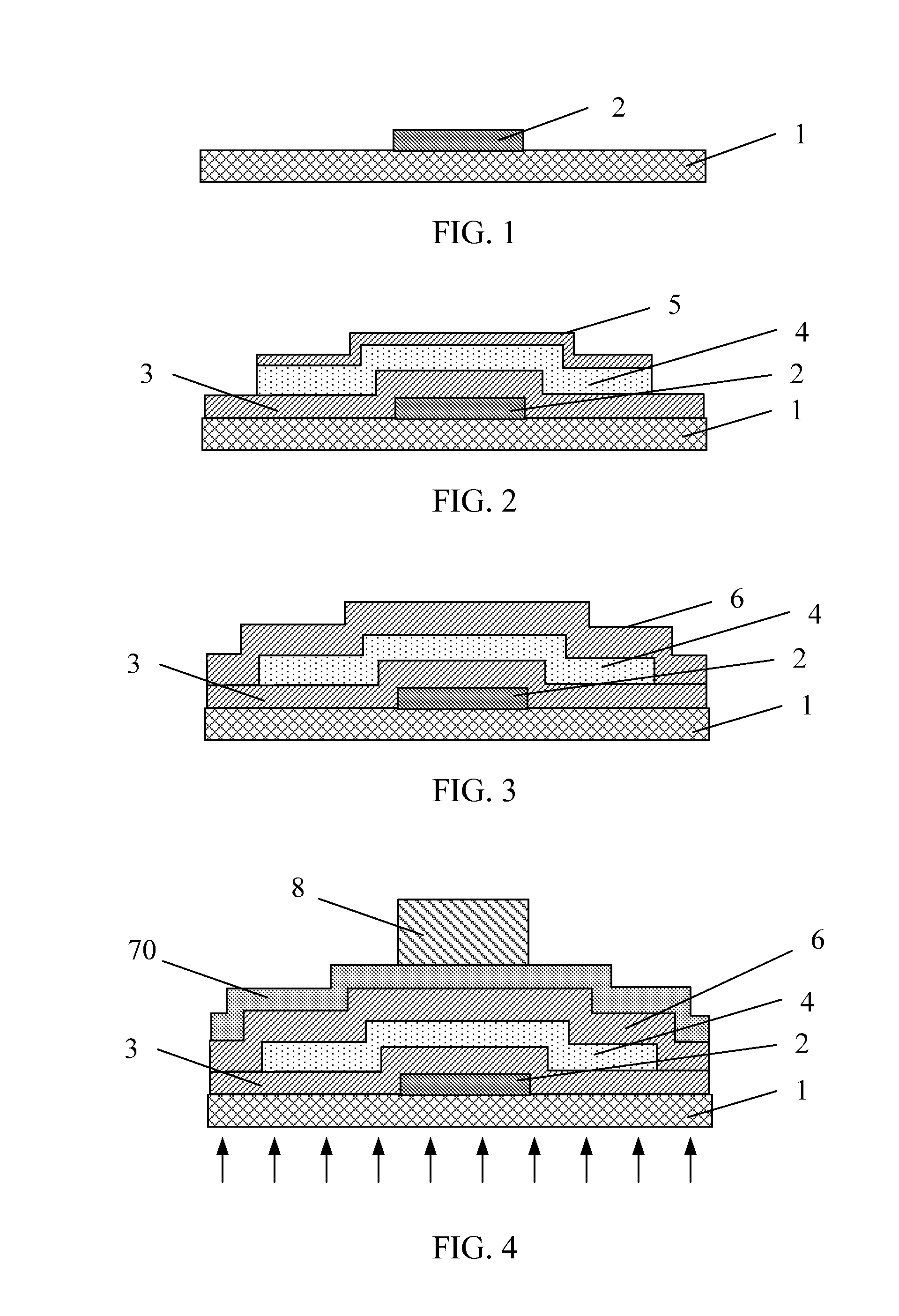
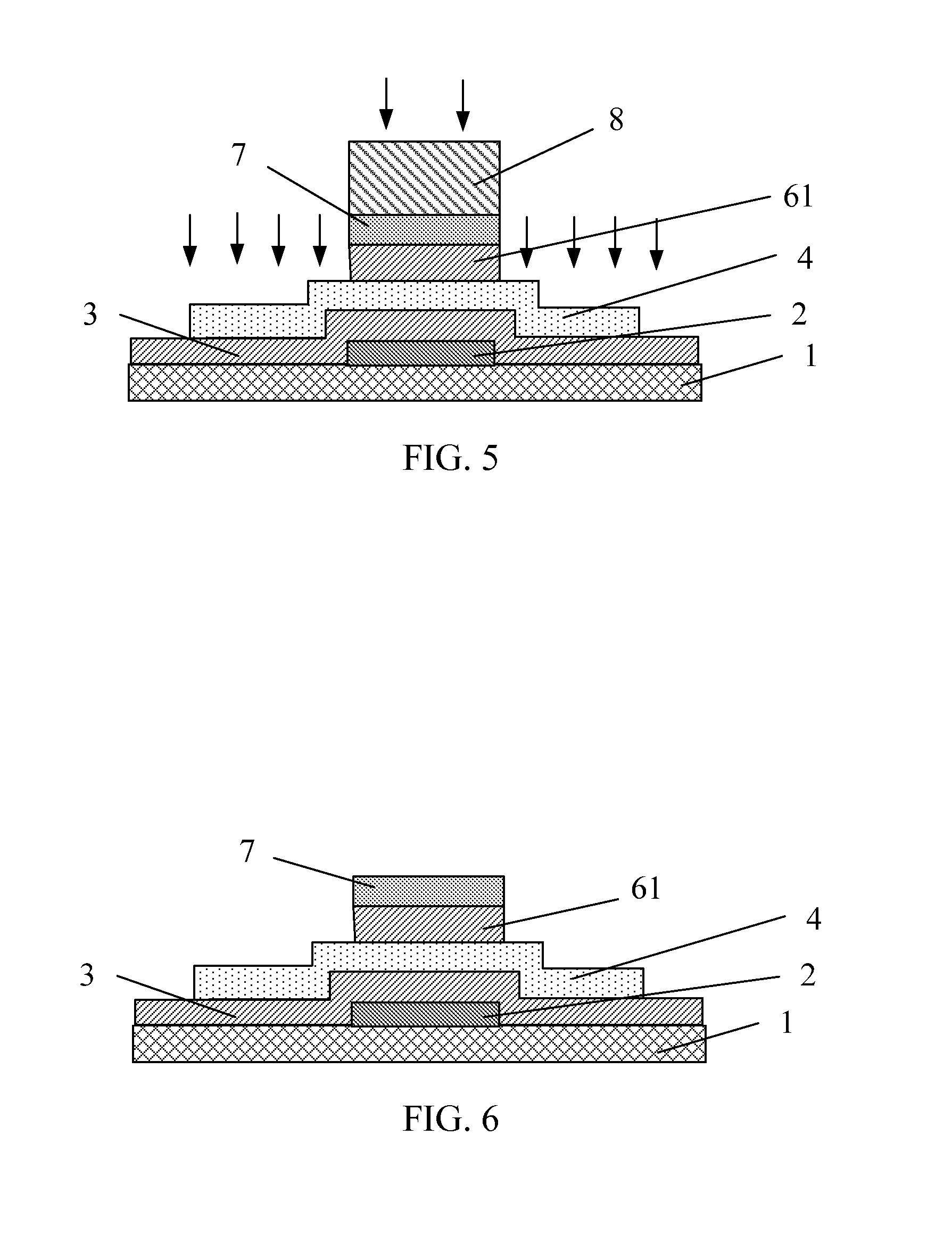
[0030]In the prior art, the top gate electrode and bottom gate electrode of a dual-gate thin film transistor cannot be aligned with each other, accurately, due to its manufacturing process. This may result in a large parasitic capacitance in the transistor, which will impact the performance of the transistor. According to the present invention, a self-aligning process is used to manufacture the dual-gate thin film transistor by means of a light-tight design. In an example of the present invention, the light-tight design is utilized for manufacturing the bottom gate electrode. For example, a light-tight material may be used to form a light-tight bottom gate electrode. On the other hand, the light-transmission design is utilized for manufacturing the substrate, the top gate electrode and layers between the top gate electrode and the bottom gate electr...
PUM
 Abstract
Description
Claims
Application Information