Method for manufacturing silicon substrate and silicon substrate
Active Publication Date: 2013-11-28
SHIN-ETSU HANDOTAI CO LTD
View PDF2 Cites 2 Cited by
Summary
Abstract
Description
Claims
Application Information
AI Technical Summary
This helps you quickly interpret patents by identifying the three key elements:
Problems solved by technology
Method used
Benefits of technology
Benefits of technology
[0045]As described above, according to the present invention, it is possible to manufacture the high-quality silicon substrate hav
Problems solved by technology
However, the size of the oxide precipitates is very small; therefore TZDB (Time Zero Dielectric Breakdown) characteristics as one of oxide dielectric breakdown voltage characteristics or device characteristics are not decreased on a shipping stage.
Moreover, when the above-described BMD is generated on the silicon substrate surface which is a device active region, device characteristics such as junction leakage are adversely affected but, on the other hand, if the BMD is present in a bulk other than the device active region, the BMD functions as a gettering site where a metal
Method used
Image
Click on the blue label to locate the original text in one second.
Reading with bidirectional positioning of images and text.
Examples
Example
EXAMPLE
[0082]The present invention will now be more specifically described based on an example and comparative examples, but the present invention is not restricted thereto.
Example
Example, Comparative Example 1
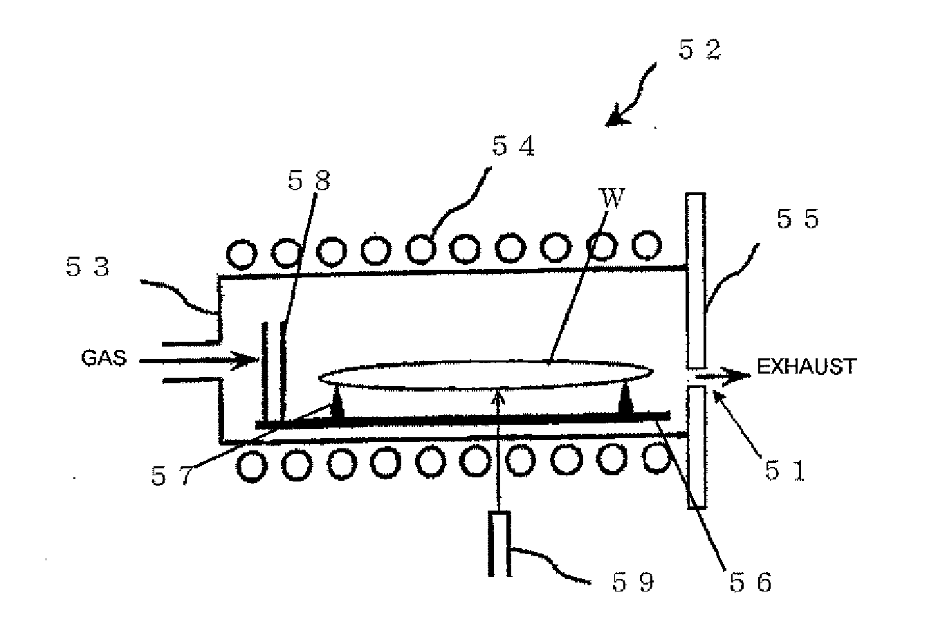
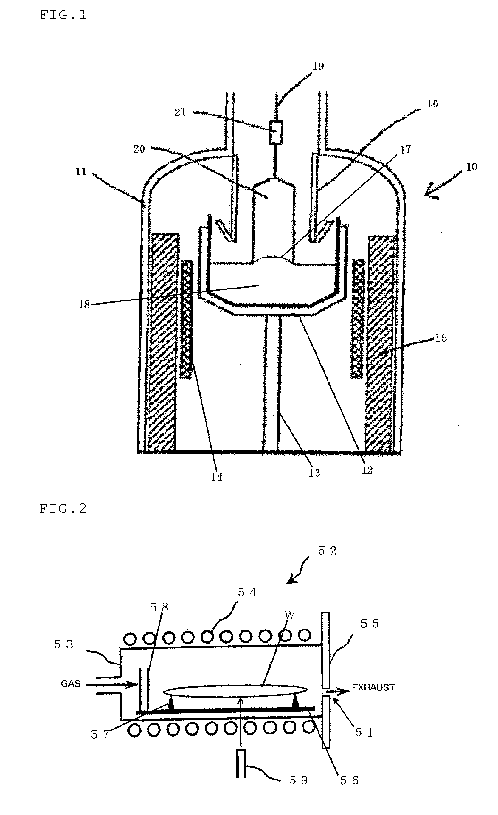
[0083]With the silicon single crystal pulling apparatus shown in FIG. 1, an N-region silicon single crystal ingot (a diameter: 12 inches (300 mm), an orientation: , a conductivity type: p type) was grown while a transverse magnetic field was applied based on the MCZ method, and silicon single crystal wafers sliced from this ingot were each subjected to a heat treatment (a rapid heat treatment) at first temperatures of 1250° C., 1290° C., 1320° C., and 1350° C. for 10 seconds with the rapid-heating and rapid-cooling apparatus (Helios manufactured by Mattson in this example) shown in FIG. 2. In this rapid heat treatment, Ar, N2, and HN3 / Ar were used as the atmosphere.
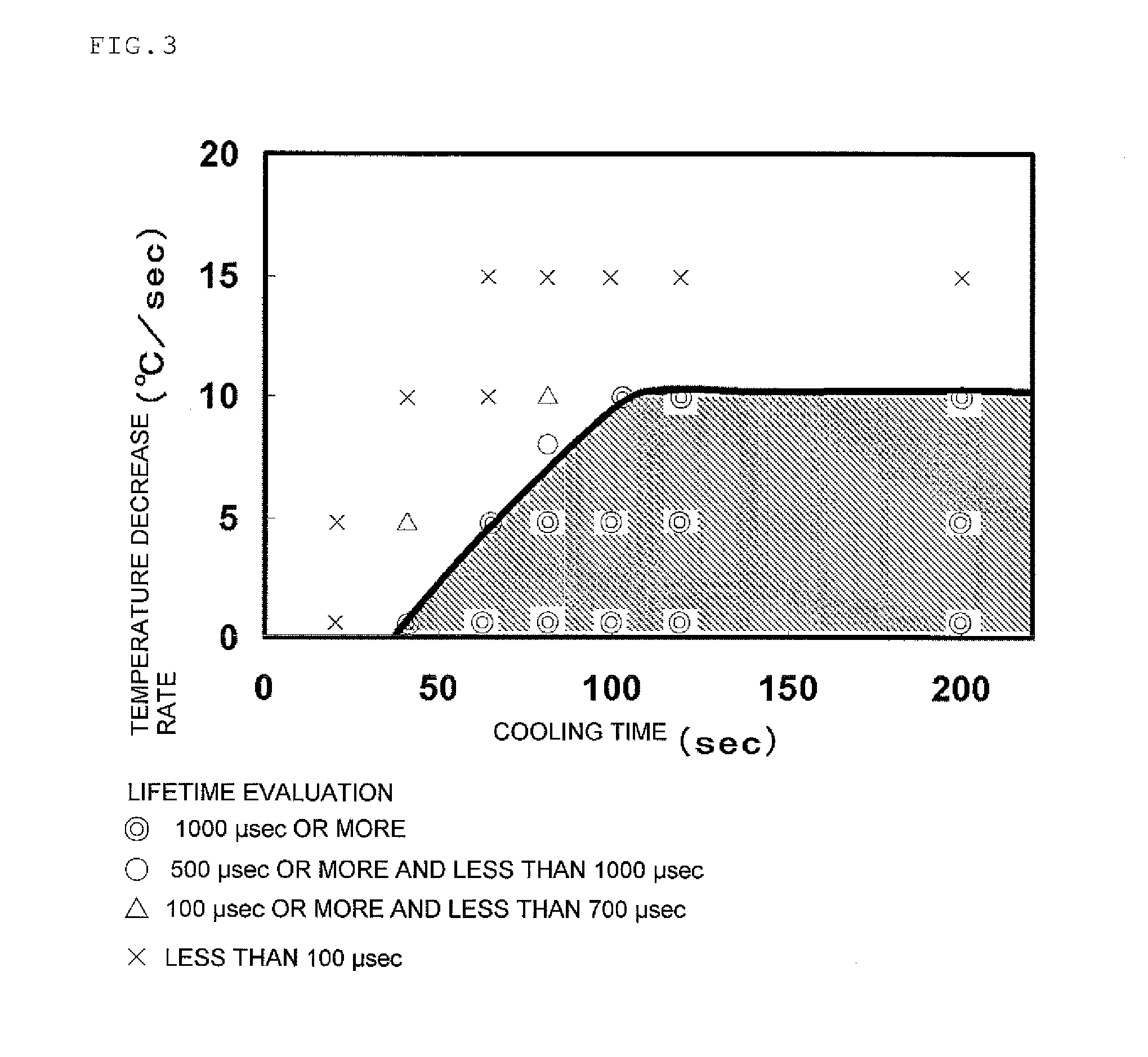
[0084]Subsequently, the first temperature decrease process from the first temperature to a second temperature was performed at a temperature decrease rate of 30° C. / sec. At this time, the second temperature was set to each of 900° C., 800° C., 700° C., 600° C., and 500° C. Then, in the second...
Example
Comparative Example 2
[0096]With the silicon single crystal pulling apparatus shown in FIG. 1, an N-region silicon single crystal ingot (a diameter: 12 inches (300 mm), an orientation: , a conductivity type: p type) was grown while a transverse field was applied based on the MCZ method, and silicon single crystal wafers sliced from this ingot were each subjected to a heat treatment (a rapid heat treatment) at first temperatures of 1250° C., 1290° C., 1320° C., and 1350° C. for 10 seconds with the rapid-heating and rapid-cooling apparatus (Helios manufactured by Mattson in this example) shown in FIG. 2. In this rapid heat treatment, Ar and HN3 / Ar were used as the atmosphere.
[0097]Subsequently, the temperature was decreased from each heat treatment temperature to a normal temperature at a temperature decrease rate of 30° C. / sec without performing the two-step temperature decrease. Then, the wafer surface was polished for approximately 5 μm.
[0098]RIE defects in a wafer surface layer of ...
PUM
Abstract
A method for manufacturing a silicon substrate, including: performing a rapid heat treatment to a silicon substrate with a rapid-heating and rapid-cooling apparatus by maintaining the silicon substrate at a temperature that is higher than 1300° C. and not greater than a silicon melting point for 1 to 60 seconds, the silicon substrate being sliced from a silicon single crystal ingot grown by the Czochralski method; performing a first temperature decrease process down to a temperature in the range of 600 to 800° C. at a temperature decrease rate of 5 to 150° C./sec; and performing a second temperature decrease process in such a mariner that a cooling time of X seconds and a temperature decrease rate of Y° C./sec meet Y≦0.15X−4.5 when X<100 and meet Y≦10 when X≧100.
Description
TECHNICAL FIELD[0001]The present invention relates to a method for manufacturing a silicon substrate in which a denuded zone (which will be referred to as a DZ layer hereinafter) having no grown-in oxide precipitate, no grown-in defect and no RIE defect (a defect that can be detected by RIE) is formed from a substrate surface to a given depth and to a silicon substrate manufactured by this method.BACKGROUND ART[0002]In recent years, with a shrinking device for high integration of a semiconductor circuit, a demand for quality of silicon single crystal fabricated by a Czochralski method (which will be referred to as a CZ method hereinafter) that serves as a substrate of this circuit has been increased.[0003]At the time of growing the silicon single crystal by the CZ method, oxygen of approximately 10 to 20 ppma (JEIDA: a conversion factor provided by Japan Electronic Industry Development Association is used) is usually dissolved into a melt from a quartz crucible and taken into the si...
Claims
Application Information
Patent Timeline
Application Date:The date an application was filed.
Publication Date:The date a patent or application was officially published.
First Publication Date:The earliest publication date of a patent with the same application number.
Issue Date:Publication date of the patent grant document.
PCT Entry Date:The Entry date of PCT National Phase.
Estimated Expiry Date:The statutory expiry date of a patent right according to the Patent Law, and it is the longest term of protection that the patent right can achieve without the termination of the patent right due to other reasons(Term extension factor has been taken into account ).
Invalid Date:Actual expiry date is based on effective date or publication date of legal transaction data of invalid patent.

