Method for manufacturing organic el display and organic el display

a technology of organic el and manufacturing method, which is applied in the manufacture of electrode systems, discharge tubes luminescent screens, electric discharge tubes/lamps, etc., can solve the problems of plasma generation imposing electric damage on electric circuits, film roughening on the surface, and possible white turbidity roughening, etc., to achieve the effect of reducing the generation of white turbidity, enhancing manufacturing quality, and manufacturing yield

Active Publication Date: 2013-12-05
JOLED INC
View PDF2 Cites 3 Cited by
  • Summary
  • Abstract
  • Description
  • Claims
  • Application Information

AI Technical Summary

Benefits of technology

[0010]There is a need for the present invention to provide an improved method for manufacturing an organic EL display, allowing suppression of the adverse effect of an electrification charge that is possibly generated in film deposition treatment in the manufacturing process, and to provide an organic EL display manufactured by the method.
[0012]In the method for manufacturing an organic EL display based on this configuration, the protective electrode that is electrically connected to the common electrode and the outer-peripheral electrode are formed before the film deposition treatment involving electrification of the substrate. Therefore, even when a film is charged in the film deposition treatment, the electrification charge flows toward the outside of the effective area due to a charge flow to the protective electrode and the outer-peripheral electrode. This avoids the occurrence of accumulation of the electrification charge at a certain position in the effective area.
[0013]According to the embodiment of the present invention, the accumulation of the electrification charge at a certain position in the effective area is avoided. Therefore, even if film deposition treatment involving electrification such as CVD deposition by use of plasma treatment is carried out in the manufacturing process for an organic EL display, it is possible to suppress generation of white turbidity at a certain position in the effective area attributed to the electrification charge generated in the film deposition treatment. Moreover, the charge flow toward the outside of the effective area can also avoid electric damage to electric circuits included in the organic EL display. Consequently, an organic EL display free from the occurrence of white turbidity and electric damage can be manufactured, which allows enhancement in the manufacturing quality, manufacturing yield, and so forth.

Problems solved by technology

This charge accumulation causes film roughening on the surface of the protective film, and this film roughening looks white turbidity.
Furthermore, the plasma generation possibly imposes electric damage on electric circuits such as a thin film transistor (hereinafter, referred to as a “TFT”) circuit included in the organic EL display.

Method used


Image

  • Method for manufacturing organic el display and organic el display
  • Method for manufacturing organic el display and organic el display
  • Method for manufacturing organic el display and organic el display

Examples


first embodiment

[0034]Initially, the schematic structure of an organic EL display will be described below.

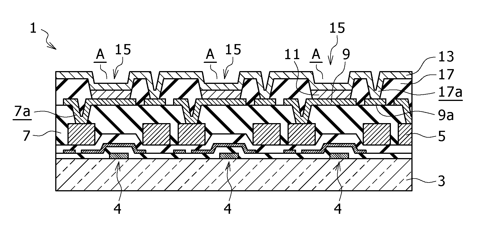
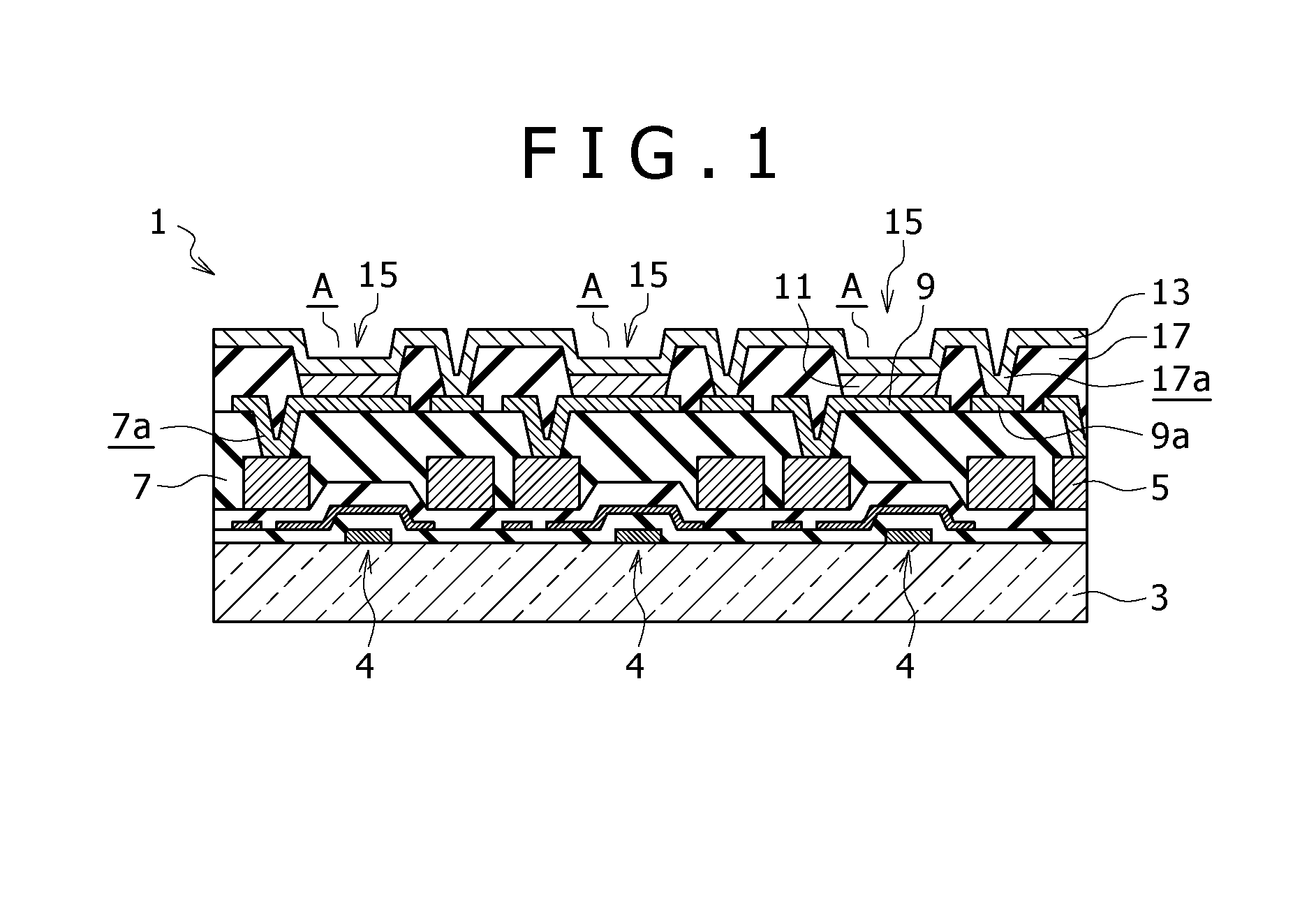
[0035]FIG. 1 is a major-part sectional view showing one example of the schematic structure of the display area of the organic EL display. In this example, the schematic structure of an active-matrix organic EL display in which organic EL elements are arranged as light-emitting elements is shown.

[0036]An organic EL display 1 of this example includes TFTs 4 in the respective pixels over a substrate 3. Over the substrate 3 on which the TFTs 4 are formed, interconnects 5 connected to the sources and drains of the TFTs 4 are formed, and a planarization insulating film 7 is provided to cover these interconnects 5. The TFT 4 is not limited to the bottom-gate TFT shown in FIG. 1 but may be a top-gate TFT. The gate electrodes of the TFTs 4 are connected to a scan circuit.

[0037]In each of pixel apertures A over this planarization insulating film 7, an organic EL element 15 arising from stacking of a lowe...

second embodiment

[0092]FIG. 6 is an explanatory diagram showing another example of a manufacturing step for an organic EL display according to a second embodiment of the present invention.

[0093]In the manufacturing of the organic EL display of this example, a metal layer (composed of e.g. a TiAl-based alloy) serving as the interconnect 5 is deposited as a pattern on the substrate 3, and the planarization insulating film 7 is deposited thereon. Furthermore, the auxiliary interconnect 9a is formed, and the upper electrode 13 is formed on the top surface side of the auxiliary interconnect 9a with the intermediary of the insulating film 17. It will be possible that the upper electrode 13 is formed of e.g. a blanket film of magnesium-silver (MgAg). Moreover, the protective film 10 for protecting the entire substrate is deposited by CVD to cover the whole of the top surface side of these layers.

[0094]However, the protective film 10 deposited by CVD will be charged due to plasma treatment. Such charging sh...

third embodiment

[0102]FIG. 8 is a major-part sectional view showing another example of the schematic structure of the display area of an organic EL display.

[0103]In the organic EL display of this example, a multilayer structure 30 obtained by sequentially stacking a cathode auxiliary interconnect 31, an interlayer insulating film 32, a source metal layer 33, a planarization film 34, an ITO layer 35, and a bank layer 36 is formed on the substrate 3. This multilayer structure 30 is formed on the light-emission area 21. A cathode 37 is deposited on the multilayer structure 30. The interlayer insulating film 32 electrically isolates data lines Idat and scan lines Vsel from the cathode auxiliary interconnect 31. On the interlayer insulating film 32, the source metal layer 33 patterned in the same step as that for the data lines Idat and the scan lines Vsel is formed into an island shape. The source metal layer 33 is electrically connected to the cathode auxiliary interconnect 31 via contact holes h5 ope...


PUM


Abstract

A method for manufacturing an organic electroluminescence display including multilayer structures that are each formed in a respective one of pixel areas in an effective area of a substrate and are each formed by a lower electrode, an organic layer, and an upper electrode, the organic electroluminescence display having a common electrode that electrically connects the pixel areas, the method including the steps of: forming a protective electrode and an outer-peripheral electrode that are electrically connected to the common electrode; forming the multilayer structures; and carrying out film deposition treatment involving electrification of the substrate.

Description

CROSS REFERENCES TO RELATED APPLICATIONS[0001]This application is a continuation of U.S. patent application Ser. No. 12 / 140,775 filed Jun. 17, 2008, the entirety of which is incorporated herein by reference to the extent permitted by law. The present invention contains subject matter related to Japanese Patent Application JP 2007-177992 filed in the Japan Patent Office on Jul. 6, 2007, the entire contents of which being incorporated herein by reference to the extent permitted by law.BACKGROUND OF THE INVENTION[0002]1. Field of the Invention[0003]The present invention relates to a method for manufacturing an organic electroluminescence (EL) display including organic EL elements and an organic EL display obtained by the manufacturing method.[0004]2. Description of the Related Art[0005]In recent years, organic EL displays including organic EL elements as light-emitting elements are attracting attention as flat displays. The organic EL display is a self-luminous flat panel display that ...

Claims


Application Information

Patent Timeline
Patent Type & Authority Applications(United States)
IPC IPC(8): H05B33/06
CPCH05B33/06H10K59/131H10K50/818H10K50/824H10K50/828H10K50/844H10K2102/3026H10K71/00H10K50/81H10K50/84H10K59/10H10K59/126H10K50/82H10K59/88H10K2102/103H10K2102/351
Inventor FUJIMURA, HIROSHIASANO, MITSURAIMAI, TOSHIAKI
Owner JOLED INC
Why Eureka
Try Eureka