Apparatus and method for reducing peak power using asynchronous circuit design technology

a technology of asynchronous circuit design and peak power, applied in logic circuits using elementary logic circuit components, instruments, computing, etc., can solve the problems of deteriorating the reliability of a semiconductor chip, increasing the probability of an operating error attributable to a high on-chip electric field on a semiconductor, and increasing the probability of an operating error attributable to a high on-chip electric field occurring on a semiconductor

Inactive Publication Date: 2013-12-05
ELECTRONICS & TELECOMM RES INST
View PDF1 Cites 0 Cited by
  • Summary
  • Abstract
  • Description
  • Claims
  • Application Information

AI Technical Summary

Benefits of technology

[0028]The controlling the partial circuits may include adjusting, by the delay element unit, a time at which the bather gate circuit unit is activated depending on delay times of the partial circuits; and being, by the bather gate circuit, activated at the time at which the bather gate circuit unit is activated and preventing, by the bather gate circuit, a switching operation of a partial circuit from propagating to other partial circuits.

Problems solved by technology

As the degree of integration of a semiconductor chip becomes higher and clock speed becomes higher, the probability of an operating error attributable to a high on-chip electric field occurring on a semiconductor is increasing.
Accordingly, in the design of semiconductor chips, the reliability of operation has become an important issue.
Such peak power generates a hot electro effect and a high current flow, thereby deteriorating the reliability of a semiconductor chip.
The hot electro effect causes a runaway current failure and a failure attributable to an electrostatic discharge, and the high current flow causes a voltage drop in the power distribution line of a semiconductor chip, thereby increasing average power and also making the supply of voltage to the semiconductor chip unstable.

Method used


Image

  • Apparatus and method for reducing peak power using asynchronous circuit design technology
  • Apparatus and method for reducing peak power using asynchronous circuit design technology
  • Apparatus and method for reducing peak power using asynchronous circuit design technology

Examples


Embodiment Construction

[0037]Embodiments of the present invention will be described with reference to the accompanying drawings in order to fully describe the present invention so that persons having ordinary knowledge in the art can easily practice the technical spirit of the present invention. It should be noted that like reference symbols are used to designate like elements throughout the drawings even when the elements are illustrated in different drawings. Furthermore, in the following description of the present invention, detailed descriptions of one or more related well-known constructions and / or one or more functions which have been deemed to make the gist of the present invention unnecessarily vague will be omitted.

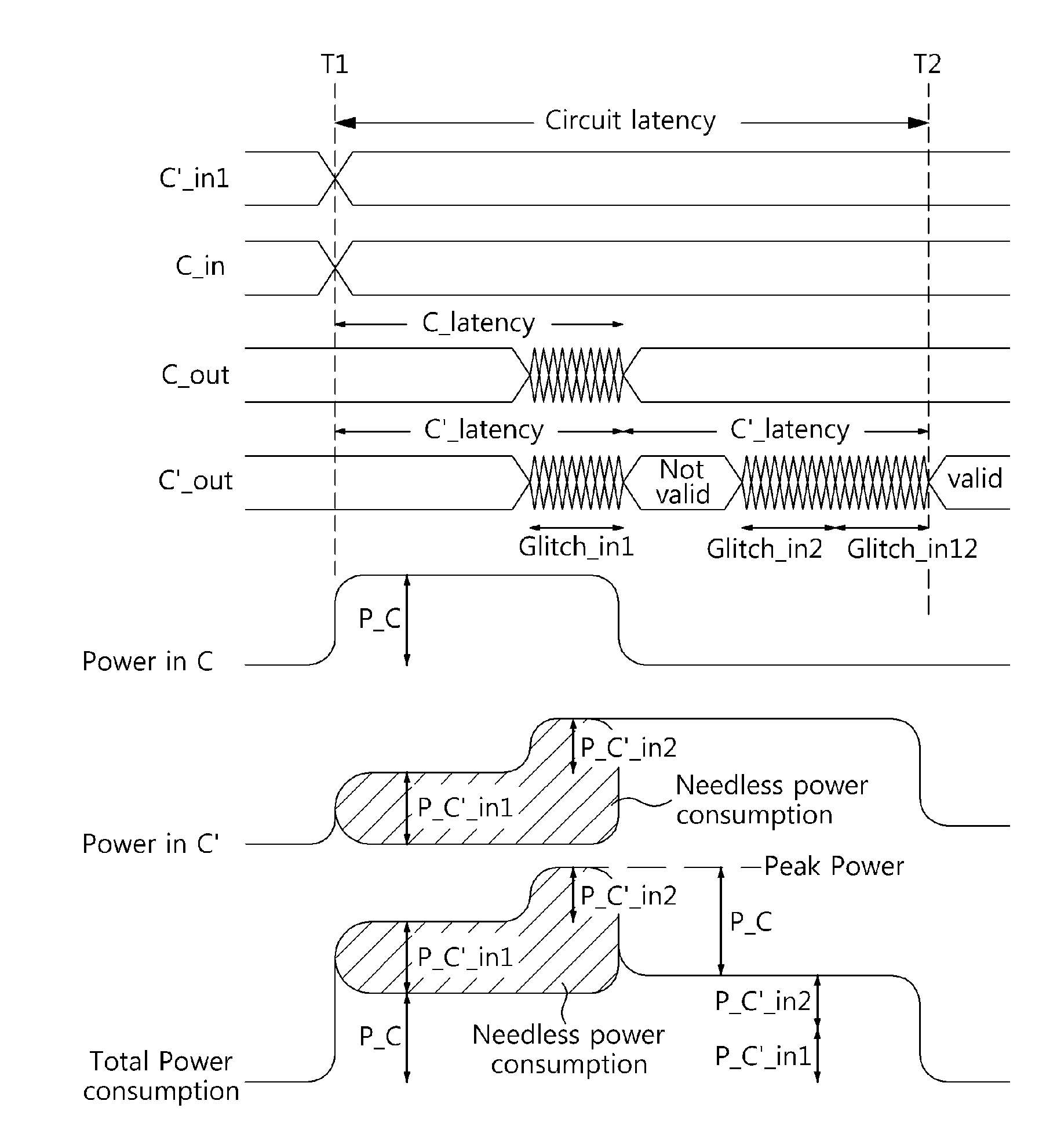
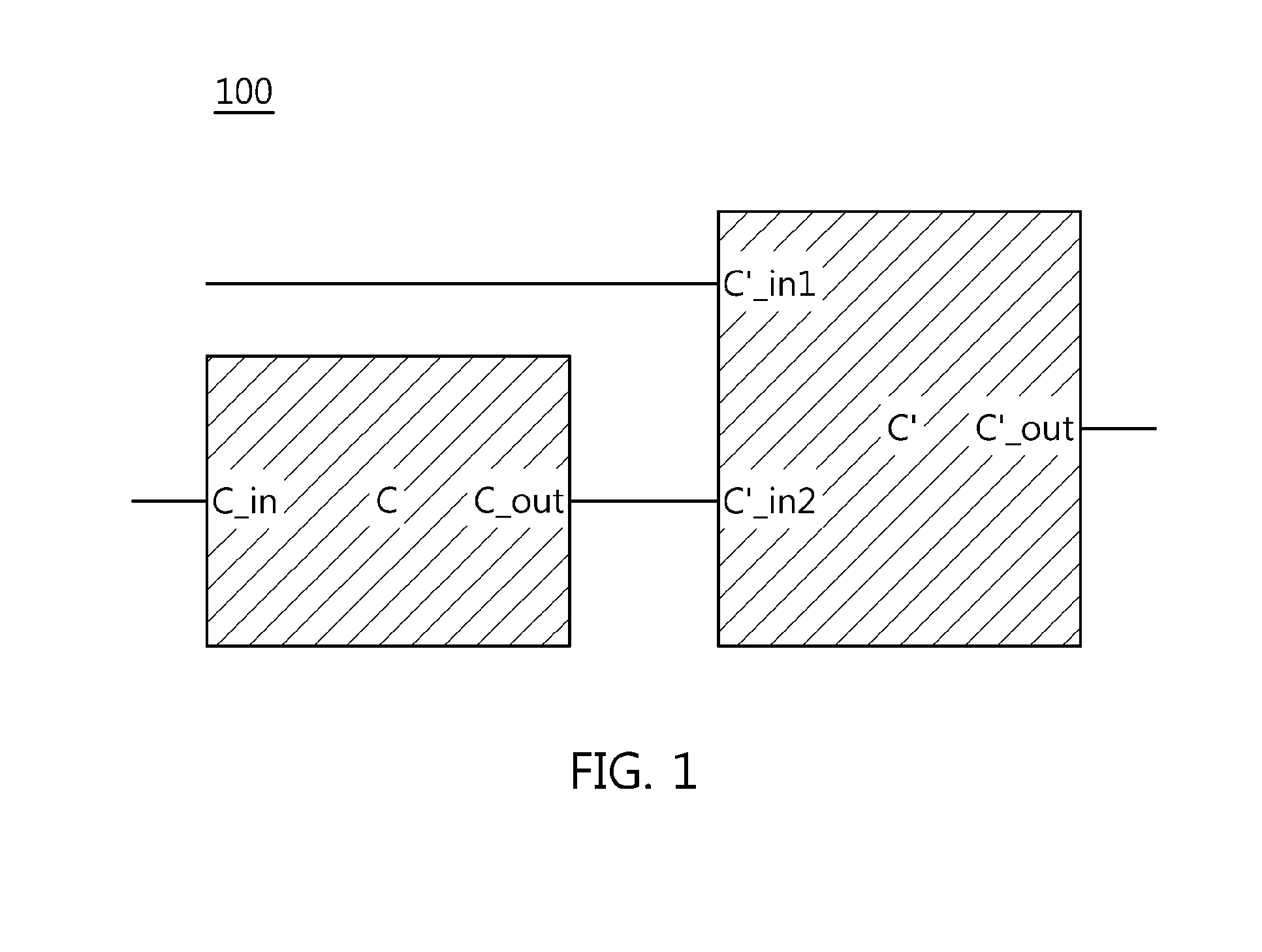
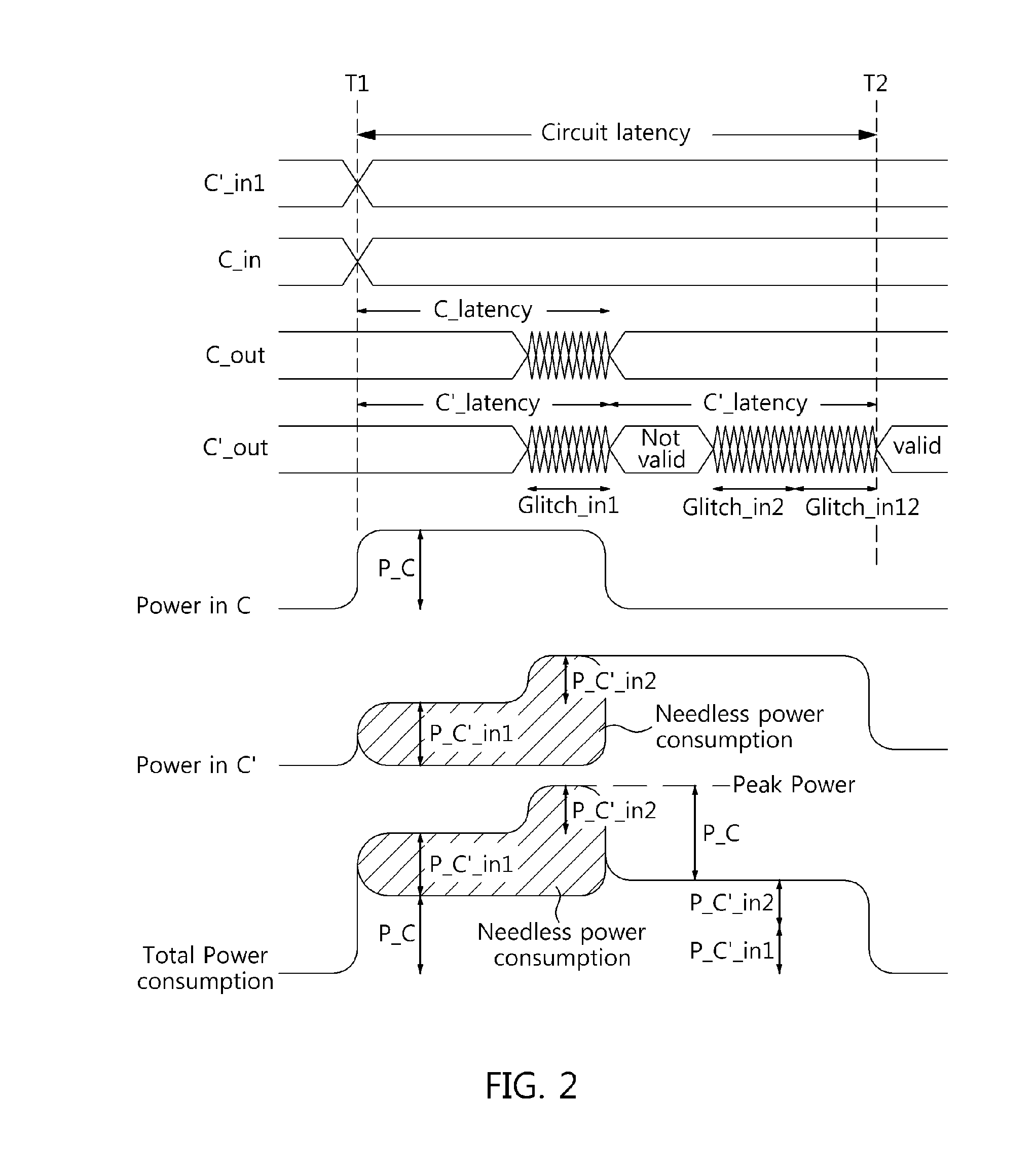
[0038]FIG. 1 is a diagram illustrating the concept of a combinational circuit

[0039]Referring to FIG. 1, a general digital circuit 100 includes combinational circuits C and C′, which receive inputs from the outside. The combinational circuit C′ includes two input ports, and receives an ...


PUM


Abstract

Disclosed herein are an apparatus and method for reducing peak power using an asynchronous circuit design technology. The apparatus includes a combinational circuit unit and an asynchronous control circuit unit. The combinational circuit unit divides a combinational circuit into a plurality of partial circuits based on the depth of input and output. The asynchronous control circuit unit controls the combinational circuit so that the switching operations of the partial circuits are performed in an asynchronous manner according to temporal order and so that a switching operation is not performed in other partial circuits when a switching operation is performed in a partial circuit.

Description

CROSS REFERENCE TO RELATED APPLICATION[0001]This application claims the benefit of Korean Patent Application No. 10-2012-0058247, filed on May 31, 2012, which is hereby incorporated by reference in its entirety into this application.BACKGROUND OF THE INVENTION[0002]1. Technical Field[0003]The present invention relates generally to an apparatus and method for reducing peak power using an asynchronous circuit design technology and, more particularly, to an apparatus and method that reduce peak power and average power by applying an asynchronous circuit design technology to a combinational circuit included in a digital circuit.[0004]2. Description of the Related Art[0005]As the degree of integration of a semiconductor chip becomes higher and clock speed becomes higher, the probability of an operating error attributable to a high on-chip electric field occurring on a semiconductor is increasing.[0006]Accordingly, in the design of semiconductor chips, the reliability of operation has bec...

Claims


Application Information

Patent Timeline
Patent Type & Authority Applications(United States)
IPC IPC(8): G06F17/50
CPCG06F17/5072G06F30/327G06F2119/06H03K19/173G06F30/392G06F30/373G06F2119/12
Inventor KIM, SUNG-NAMSHIN, CHI-HOONSONG, SUNG-GUNKIM, SEONG-WOON
Owner ELECTRONICS & TELECOMM RES INST
Why Eureka
Try Eureka