Semiconductor memory device

a memory device and semiconductor technology, applied in the direction of information storage, static storage, digital storage, etc., can solve problems such as unnecessary current consumption, and achieve the effect of preventing current consumption

Active Publication Date: 2013-12-19
SK HYNIX INC
View PDF0 Cites 1 Cited by
  • Summary
  • Abstract
  • Description
  • Claims
  • Application Information

AI Technical Summary

Benefits of technology

[0037]An embodiment of the present invention is directed to a semiconductor memory device that may prevent current consumption caused by unnecessary toggling in a pre-decoding circuit which selects a half page by using some bits of a row address.

Problems solved by technology

Therefore, although it does not have to select a half page, initializing the first pre-decoding signal LAXD0> and the second pre-decoding signal LAXD1> to a logic low level whenever a bank is precharged after the bank is activated requires unnecessary toggling, which means unnecessary current consumption.

Method used


Image

  • Semiconductor memory device
  • Semiconductor memory device
  • Semiconductor memory device

Examples


Embodiment Construction

[0046]Exemplary embodiments of the present invention will be described below in more detail with reference to the accompanying drawings. The present invention may, however, be embodied in different forms and should not be construed as limited to the embodiments set forth herein. Rather, these embodiments are provided so that this disclosure will be thorough and complete, and will fully convey the scope of the present invention to those skilled in the art. Throughout the disclosure, like reference numerals refer to like parts throughout the various figures and embodiments of the present invention.

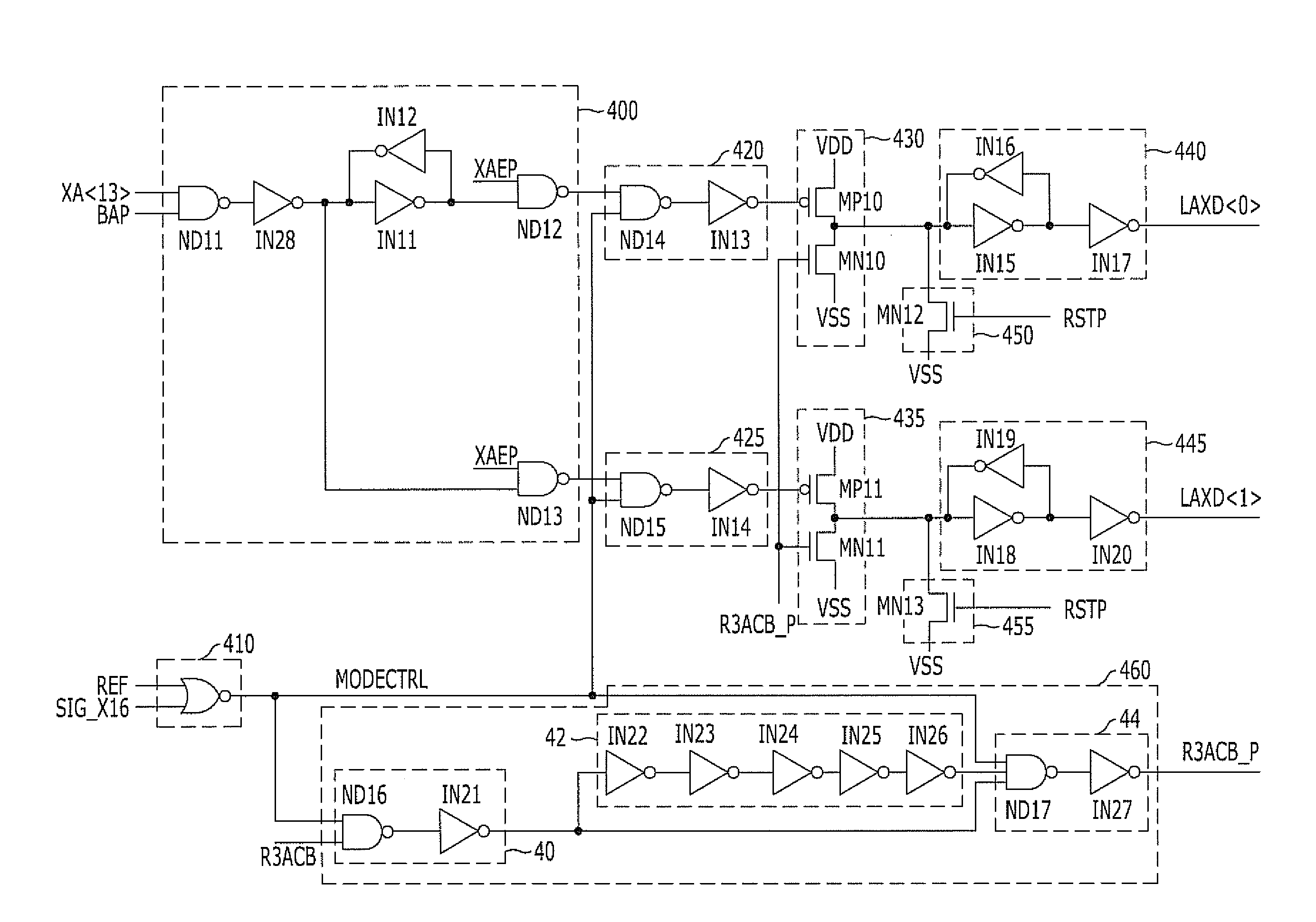
[0047]FIG. 4 is a circuit diagram of a row pre-decoding circuit in accordance with an embodiment of the present invention. The drawing shows a unit pre-decoding circuit that corresponds to the MSB of the pre-decoder.

[0048]Referring to FIG. 4, the conventional pre-decoding circuit includes an input unit 400, a control signal generation unit 410, a first mode control unit 420, a second mode co...


PUM


Abstract

A semiconductor memory device selecting a half page based on a particular bit of a row address includes: an input unit for receiving the particular bit; a control signal generation unit for outputting a mode control signal in response to a signal related to a mode for selecting a whole page; first and second mode control units for transferring first and second output signals of the input unit corresponding to the particular bit and its inverse signal; a row precharge pulse generation unit for generating a row precharge pulse enabled in an initial period of a precharge duration; a first driving unit for pull-up/pull-down driving an output terminal corresponding to a first pre-decoding signal; a second driving unit for pull-up/pull-down driving an output terminal corresponding to a second pre-decoding signal; and first and second latch units for latching output signals of the first and second driving units.

Description

BACKGROUND[0001]1. Field[0002]Exemplary embodiments of the present invention relate to a semiconductor designing technology, and more particularly, to a low pre-decoder circuit of a semiconductor memory device.[0003]2. Description of the Related Art[0004]Semiconductor memory devices including Dynamic Random Access Memory (DRAM) devices are using a row / column addressing scheme. First, a row address is inputted from the outside to select a row, which is a word line, and then a column address is inputted from the outside to select a column of the selected row, which is a bit line.[0005]Conventionally, since there are many rows and columns, a method of decoding an address of multiple bits is being used. To taken an example of row addressing, a scheme where a pre-decoder is disposed in front of a main decoder and a word line driver to minimize the circuit area needed for a decoding circuit.[0006]Meanwhile, word lines are generally formed of polysilicon to overcome technical limitation. H...

Claims


Application Information

Patent Timeline
Patent Type & Authority Applications(United States)
IPC IPC(8): G11C7/10
CPCG11C11/406G11C11/4085G11C11/4087G11C8/10G11C7/10G11C11/4063
Inventor JUNG, TAEHYUNG
Owner SK HYNIX INC
Why Eureka
Try Eureka