Triaxial piezoelectric sensor

a piezoelectric sensor and triaxial technology, applied in the field of piezoelectric sensors, can solve the problems of limited use, fragility and structural damage, heavy weight, and hard piezoelectric materials, and achieve the effect of high sensitivity

Inactive Publication Date: 2014-01-02
CHUNG YUAN CHRISTIAN UNIVERSITY
View PDF3 Cites 6 Cited by
  • Summary
  • Abstract
  • Description
  • Claims
  • Application Information

AI Technical Summary

Benefits of technology

[0005]A major objective of the present invention is to ...

Problems solved by technology

In general, piezoelectric ceramic materials have the features of small size, fast reaction, and low power consumption, but limitations on their use include fragility and structural damage due to uneven force...

Method used


Image

  • Triaxial piezoelectric sensor
  • Triaxial piezoelectric sensor
  • Triaxial piezoelectric sensor

Examples


first embodiment

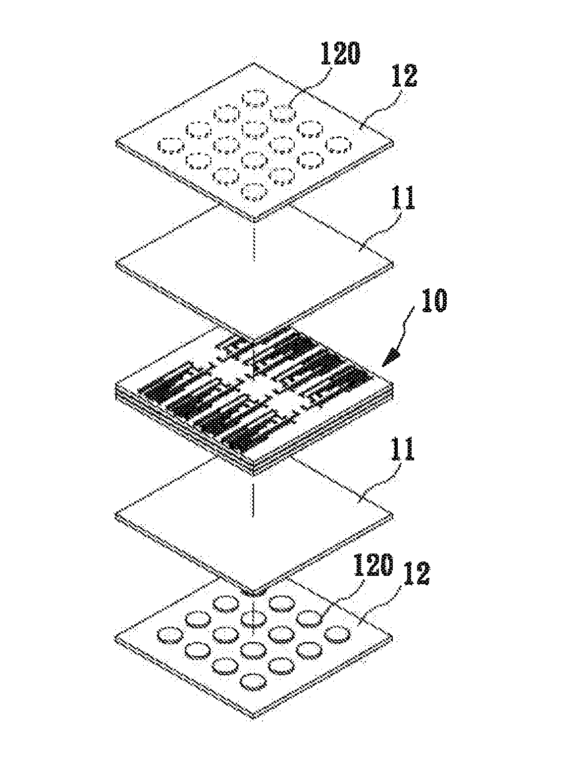
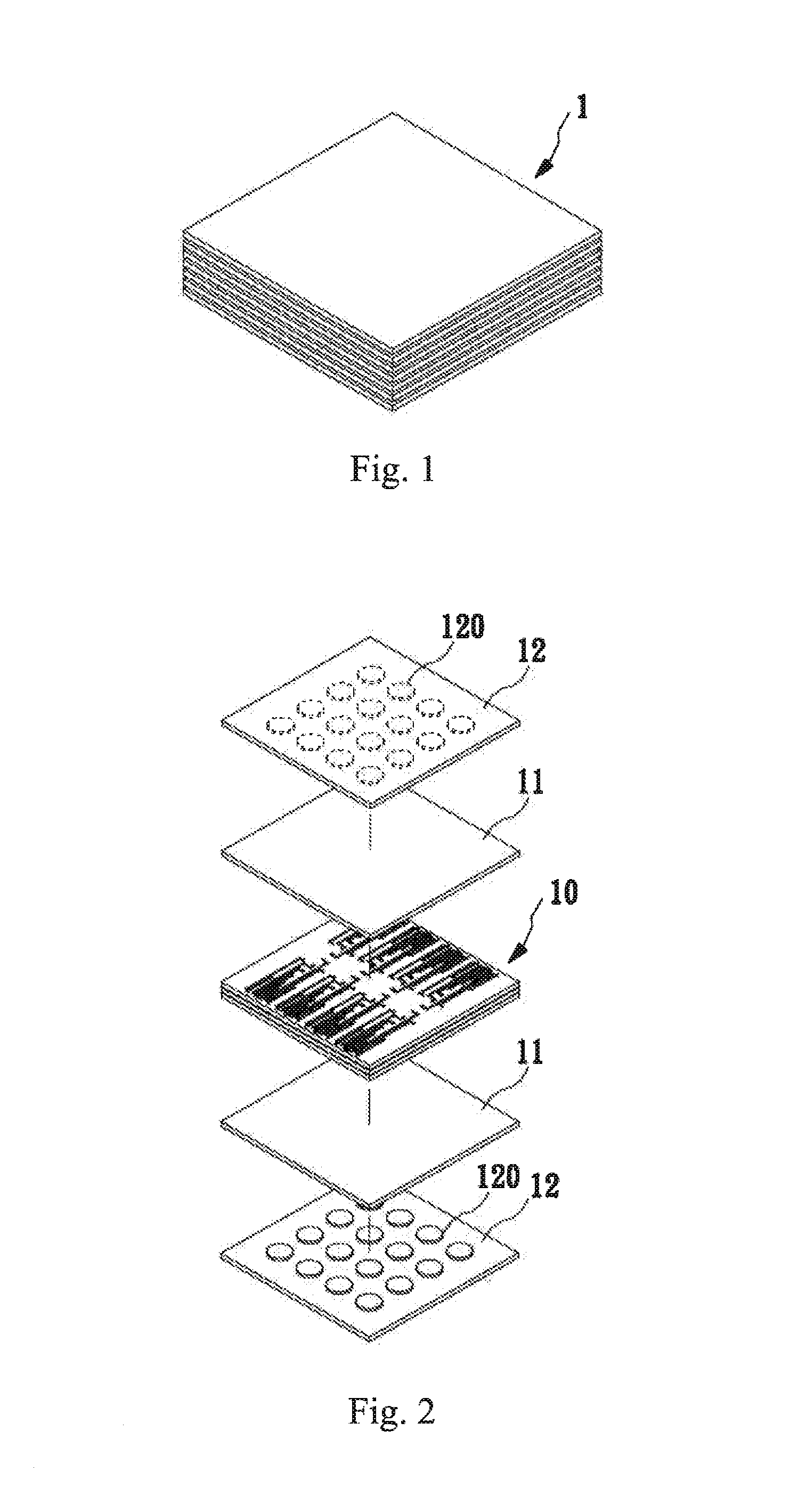
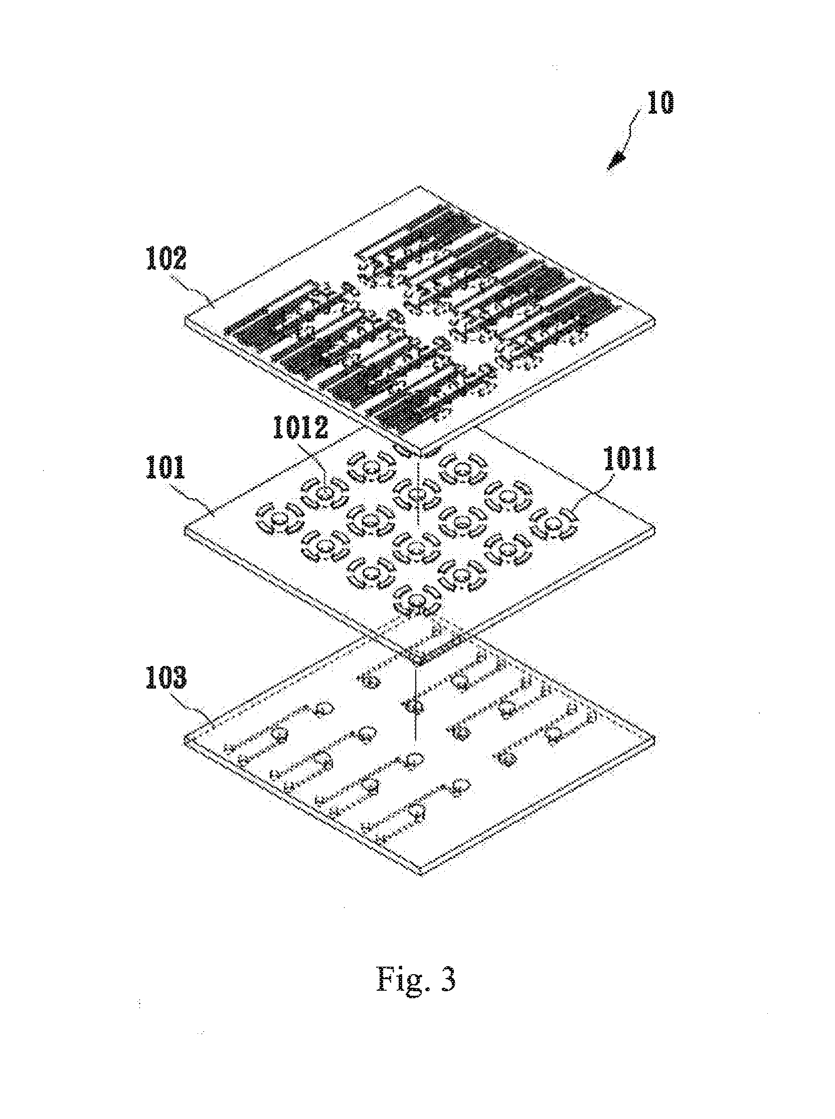
[0036]Please refer to FIG. 1 to FIG. 3. FIG. 1 is a triaxial piezoelectric sensor 1. A major sensing function of the triaxial piezoelectric sensor 1 is achieved when the sensor body 10 in the triaxial piezoelectric sensor 1 is deformed to generate an electrical signal. Please refer to FIG. 3; the sensor body 10 comprises a Polyvinylidene (PVDF) layer 101, a first line layer 102, and a second line layer 103, wherein the PVDF layer 101 is located between the first line layer 102, and the second line layer 103.

[0037]Please refer to FIG. 4A to FIG. 4D, which explain details of the PVDF layer 101. FIG. 4A illustrates a top view of the PVDF layer 101, FIG. 4B illustrates a lateral view of the PVDF layer 101, FIG. 4C illustrates a bottom view of the PVDF layer 101, and FIG. 4D illustrates the polarized directions on the dashed portion indicated in FIG. 4B. As indicated in FIG. 4A, first electrodes 1011 are located in an upper surface of the PVDF layer 101. FIG. 4C illustrates that second e...

second embodiment

[0043]In the second embodiment, the first line layer 702 and the second line layer 703 are substantially the same but only different in the opposed upper surface and bottom surface. Such an arrangement helps simplify the manufacturing process. FIG. 10A-10C respectively illustrate an upper surface, a lateral surface, and a bottom surface of the first line layer. The first line layer 702 has a plurality of first electrodes 7021 located in a bottom surface of the first line layer 702 and has a plurality of first signal lines 7022 located in an upper surface of the first line layer 702.

[0044]Because the line layer 702 and the second line layer 703 are substantially the same but only different in the opposed upper surface and bottom surface, it is proper to use FIG. 10A-10C for also illustrating the second line layer 703. For brevity, FIG. 10A-10C are also used for illustrating a bottom surface, a lateral surface, and an upper surface of the second line layer 703. The second line layer 7...

third embodiment

[0052]In the third embodiment, the third line layer 132 for the second sensor body 13a is substantially the same as the fourth line layer 133a, only having opposite upper and bottom surfaces. FIG. 16A-16C respectively illustrate an upper surface, a lateral surface, and a bottom surface of the third line layer. The third line layer 132a has a plurality of third electrical connection portions 1321a located in a bottom surface of the third line layer 1321a and has a plurality of third signal lines 1322a located in an upper surface of the third line layer 1321a.

[0053]Because the third line layer 132a of the third embodiment is substantially the same as the fourth line layer 133a, only having opposite upper and bottom surfaces, FIG. 16A-16C are also used for illustrating the fourth line layer 133a. For brevity, FIG. 16A-16C are used for illustrating a bottom surface, a lateral surface, and an upper surface of the fourth line layer 133a. The fourth line layer 133a has a plurality of four...


PUM


Abstract

A triaxial piezoelectric sensor includes a PVDF layer, a first line layer, and a second line layer. The PVDF layer has multiple first electrodes and multiple second electrodes. Each first electrodes corresponds to each second electrodes for forming directions of polarization along the X-Y-Z axes. The first line layer has multiple first electrical connection portions and multiple first signal lines. Each first electrical connection portions corresponds to each first electrodes. The second line layer has multiple second electrical connection portions and multiple second signal lines. Each second electrical connection portions corresponds to each second electrodes. The PVDF layer is sandwiched between the first line layer and the second line layer. When an external force is applied to the PVDF layer, the first signal lines and the second signal lines transmit electrical signals according to the deformation of the PVDF layer.

Description

FIELD OF THE INVENTION[0001]The present invention relates to a piezoelectric sensor, and more particularly relates to a triaxial piezoelectric sensor.BACKGROUND[0002]The piezoelectric effect the use of material deformation to convert mechanical energy to electrical energy or to convert electric energy to mechanical energy. Since the piezoelectric feature of BaTiO3 was discovered in 1942, studies on various piezoelectric materials have continued.[0003]Conventional piezoelectric materials are based on the inorganic ceramic BaTiO3 and lead ziroconate-titanate. In general, piezoelectric ceramic materials have the features of small size, fast reaction, and low power consumption, but limitations on their use include fragility and structural damage due to uneven force applied thereon.[0004]However, inorganic piezoelectric materials are hard, fragile, and heavy, and they are difficult to process into thin films or films with complicated shapes. The cost of such materials is also high.SUMMAR...

Claims


Application Information

Patent Timeline
IPC IPC(8): G01R5/28
CPCG01R5/28G01L1/16G01L5/167B06B1/0692B06B1/0644B06B1/0622H10N30/01
Inventor TING, YUNGLIN, SHEUAN-PERNGGUNAWAN, HARIYANTO
Owner CHUNG YUAN CHRISTIAN UNIVERSITY
Why Eureka
Try Eureka