Semiconductor light-emitting device

Active Publication Date: 2014-01-16
STANLEY ELECTRIC CO LTD
View PDF10 Cites 8 Cited by
  • Summary
  • Abstract
  • Description
  • Claims
  • Application Information

AI Technical Summary

Benefits of technology

[0029]According to the exemplary semiconductor light-emitting devices, the same or similar features of the device can be offered as set forth in preceding paragraphs. Thus, the disclosed subject matter can include providing small semic

Problems solved by technology

As a result, the peeling may cause a degradation of optical characteristics such as a reduction of a light-emitting intensity, color variability, a light-emitting failure and the like, and finally may cause a failure of the semiconductor light-emitting device.
Therefore, the above-described structure of the device may cause a degradation of a reliability of the semiconduc

Method used


Image

  • Semiconductor light-emitting device
  • Semiconductor light-emitting device
  • Semiconductor light-emitting device

Examples


first embodiment

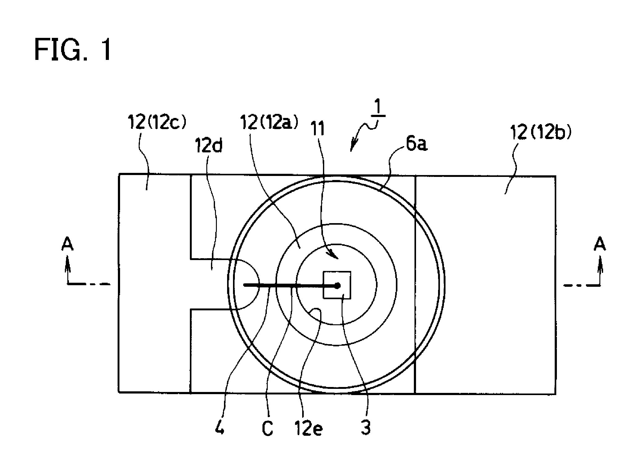
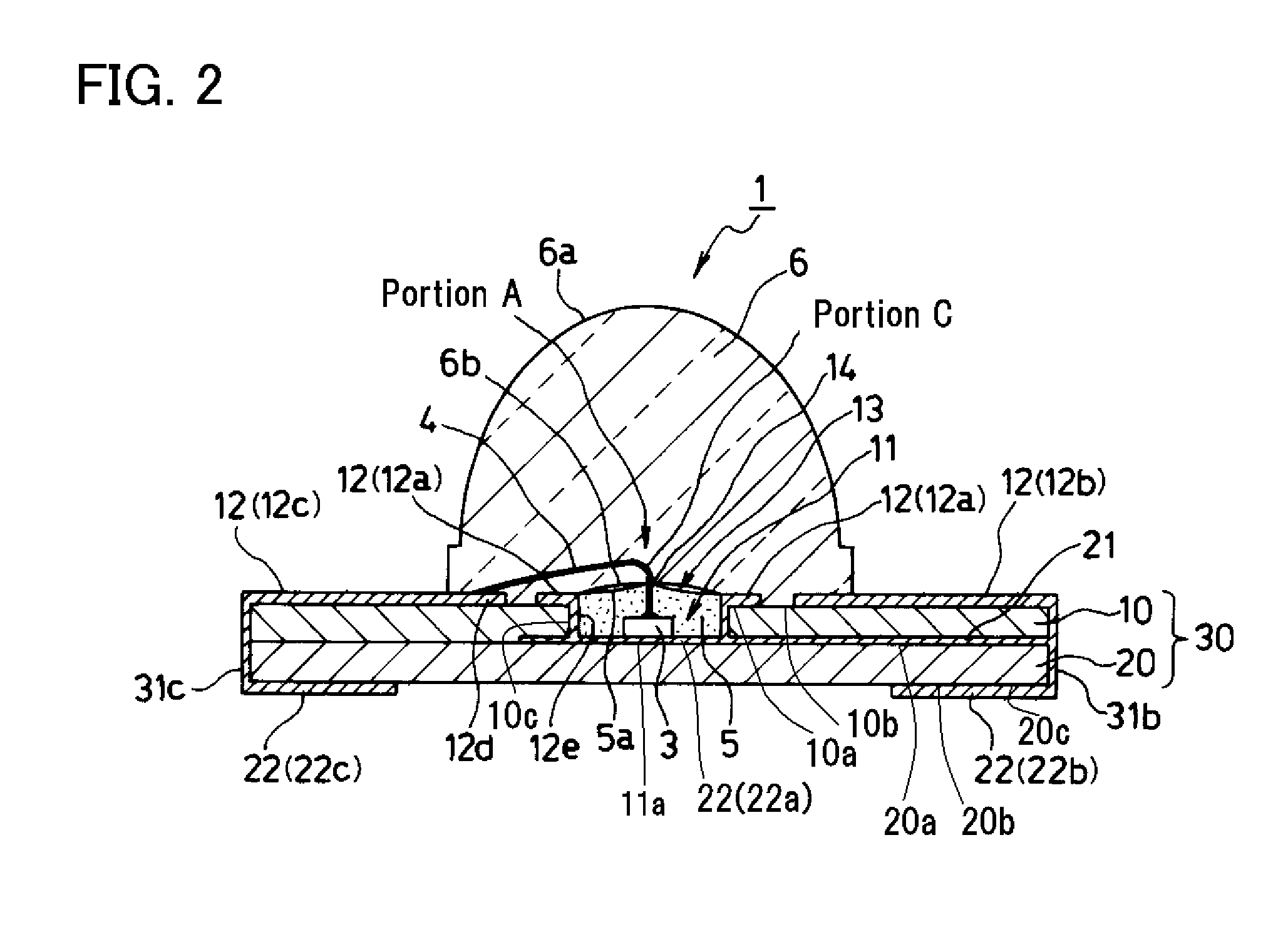
[0049]Exemplary embodiments and manufacturing methods of the disclosed subject matter will now be described in detail with reference to FIGS. 1 to 17b, in which the same or corresponding elements use the same reference marks. FIG. 1 is an enlarged top view showing a first exemplary embodiment of a semiconductor light-emitting device made in accordance with principles of the disclosed subject matter, and FIG. 2 is an enlarged side cross-sectional view taken along line A-A in FIG. 1 showing the semiconductor light-emitting device of FIG. 1.

[0050]The semiconductor light-emitting device 1 can include a base board 30 having a cavity 11 with a two layer structure made by attaching a first board 10 having a through hole (11), which is formed in a substantially rectangular tabular shape so that the through hole thereof can form the cavity 11 of the base board 30, on a top surface 20a of a second board 20, which is also formed in a substantially same rectangular tabular shape as the substant...

second embodiment

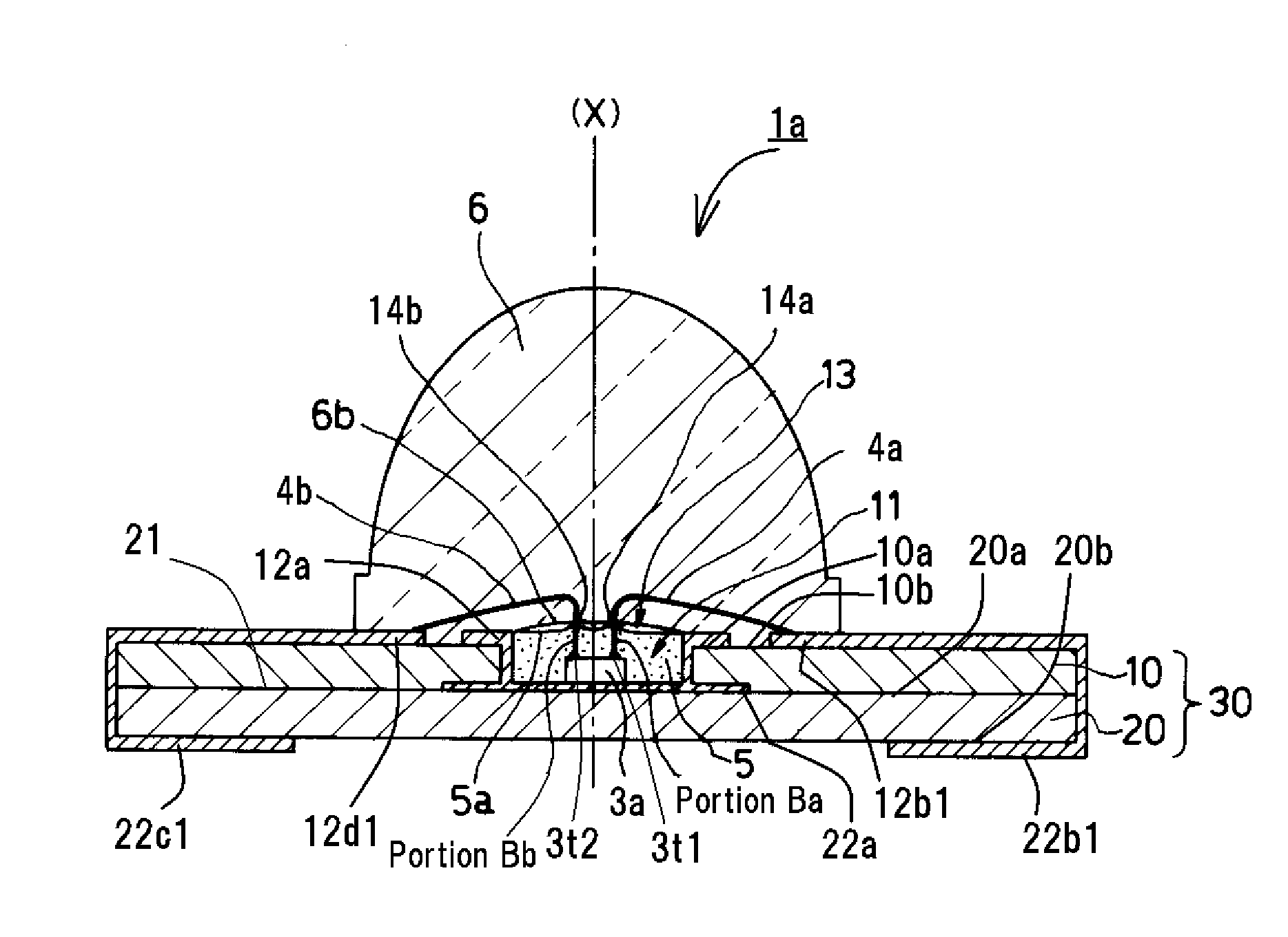
[0105]In addition, the semiconductor light-emitting device 1a of the second embodiment can also include a semiconductor light-emitting chip 3a having a first top electrode 3t1 and a second top electrode 3t2 mounted on the bottom surface of the cavity 11, the first top electrode 30 being electrically connected to the first bonding pattern 12b1 via a first bonding wire 4a, which connects the first electrode 22b1 used as the electrode of the device 1a, the second top electrode 3t2 being electrically connected to the second bonding pattern 12d1 via a second bonding wire 4b, which connect the second electrode 22c1 used as the other electrode of the device 1a to receive a power supply for emitting light from the semiconductor light-emitting chip 3a.

[0106]In the semiconductor light-emitting device 1a of the second embodiment, which is manufactured by the above-described manufacturing method, the wavelength converting material 5 can be disposed in the cavity 11, in which the top surface 5a...


PUM


Abstract

A reliable semiconductor light-emitting device can include a wavelength converting material in a cavity mounting at least one semiconductor light-emitting chip. The device can also include an encapsulating resin to cover the wavelength converting material so as to emit a wavelength-converted light using light emitted from the chip. The wavelength converting material should include a transparent resin having a large thermal expansion coefficient to maintain a high thermal resistance, and the encapsulating resin is subject to cracks due to a high transparent resin. The semiconductor device can be configured to form a space between the wavelength converting material and the encapsulating resin so that each of the encapsulating resin and the wavelength converting material cannot contact with each other even under a high temperature. Thus, the disclosed subject matter cannot stress in the encapsulating resin when the wavelength converting material expands, and therefore can provide the reliable semiconductor light-emitting device.

Description

[0001]This application claims the priority benefit under 35 U.S.C. §119 of Japanese Patent Application No. 2012-156680 filed on Jul. 12, 2012, which is hereby incorporated in its entirety by reference.BACKGROUND[0002]1. Field[0003]The presently disclosed subject matter relates to semiconductor light-emitting devices, and more particularly to surface mount semiconductor light-emitting devices with a high reliable structure, which can prevent causing cracks in encapsulating resins during / after a reflow soldering process when the semiconductor light-emitting devices are mounted on a mounting circuit board.[0004]2. Description of the Related Art[0005]Semiconductor light-emitting devices, in which a part of the light emitted from a semiconductor light-emitting chip is converted into light having a different wavelength by a phosphor and in which a mixture light including the light having the different wavelength mixed with the light emitted directly from the semiconductor light-emitting c...

Claims


Application Information

Patent Timeline
IPC IPC(8): H01L33/52
CPCH01L33/52H01L33/501H01L33/54H01L33/56H01L33/507H01L2224/48465H01L2224/8592
Inventor MORIMOTO, MAYO
Owner STANLEY ELECTRIC CO LTD
Why Eureka
Try Eureka