Method for manufacturing a component having an electrical through-connection

Active Publication Date: 2014-01-30
ROBERT BOSCH GMBH
View PDF9 Cites 12 Cited by
  • Summary
  • Abstract
  • Description
  • Claims
  • Application Information

AI Technical Summary

Benefits of technology

The present invention provides a method for manufacturing a component with a through-connection that is robust at high temperatures and avoids metal entrainment during grinding. The method includes producing an insulating trench surrounding a contact area, introducing an insulating material into the trench to create a ring-shaped insulating structure, depositing a metal material in the contact area, and removing the excess metal to create the contact hole. The contact hole is not filled with metal until the end of the manufacturing process, which prevents damage to the through-connection and allows better quality of the deposited layers. The method also allows for higher processing temperatures and greater layer thicknesses during processing.

Problems solved by technology

Since in this concept the production of the through-connections takes place at the very end of the wafer process, these approaches are also referred to as “via-last.” A critical factor, among others, in these via-last approaches is the poor quality of the insulating layer, since the deposition of insulating material in the deep holes having a high aspect ratio may be achieved only in small thicknesses due to technical reasons.
In addition, the oxides typically used as the insulating material have relatively poor oxide quality, since only deposition processes having a low maximum process temperature may be used at the end of the wafer processing.
Due to the high aspect ratio of the holes, opening the insulating layer at the base of the holes is also particularly difficult.
Lastly, the deposition of a diffusion barrier, which is typically carried out prior to the metal deposition, is also very difficult technically due to the high aspect ratio and the depth of the holes.
In these typical via-middle processes, differences in the thermal coefficients of expansion of the metals used and of the silicon substrate may result in damage to the previously applied TSV structures during the back-end processes.
In addition, the grinding process has proven to be very difficult, since various materials such as silicon, oxide, barrier material, and metal must be ground at the same time; furthermore, metal smearing over the oxide insulating surface must be avoided to the greatest extent possible.

Method used


Image

  • Method for manufacturing a component having an electrical through-connection
  • Method for manufacturing a component having an electrical through-connection
  • Method for manufacturing a component having an electrical through-connection

Examples


Embodiment Construction

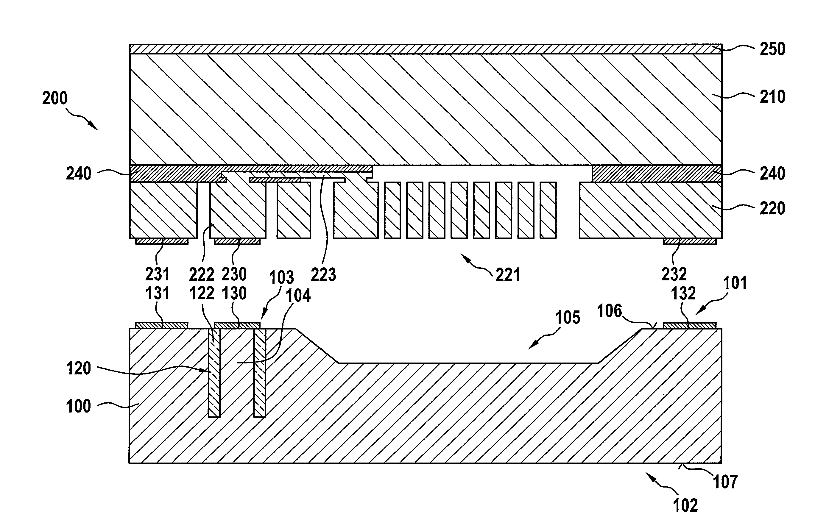
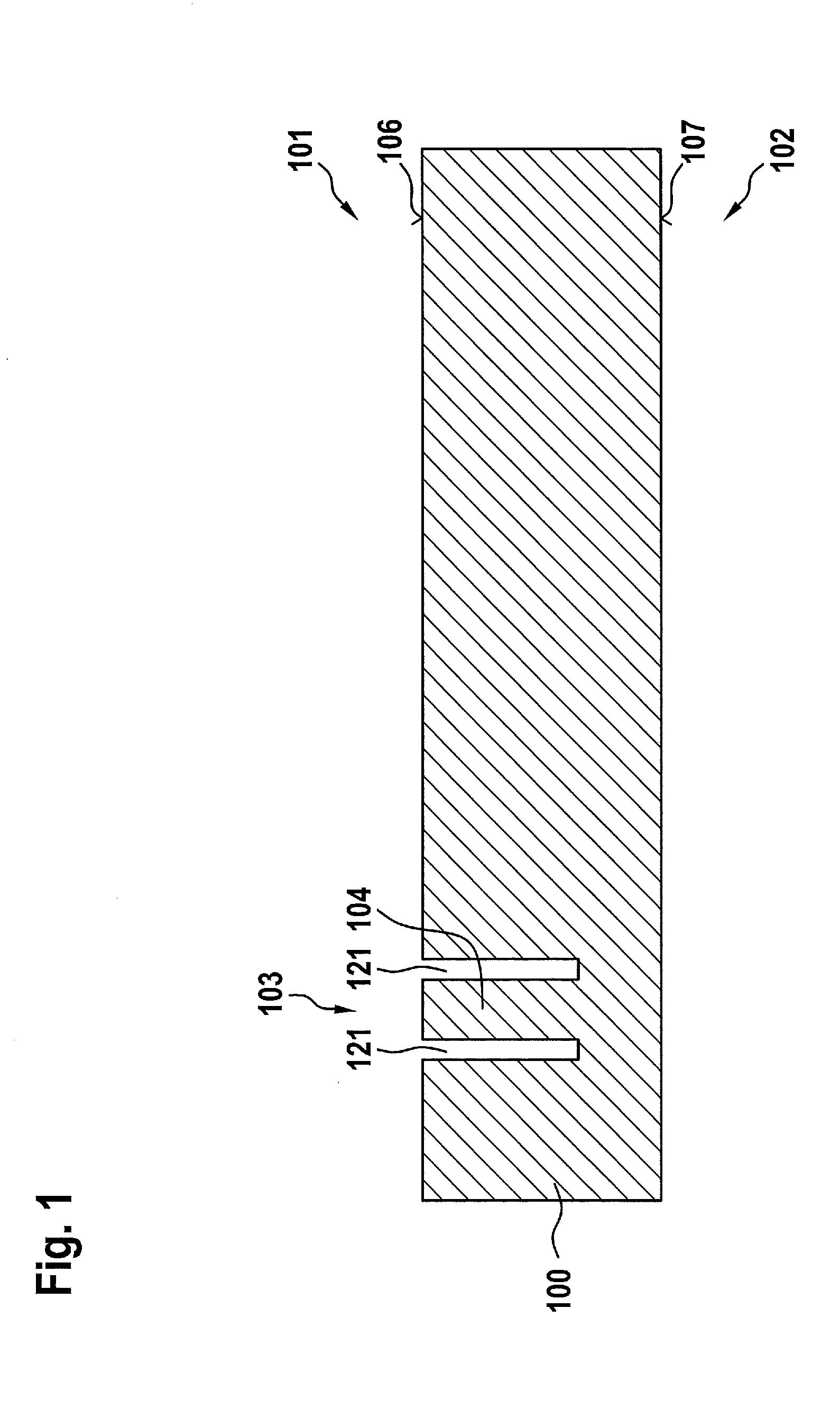
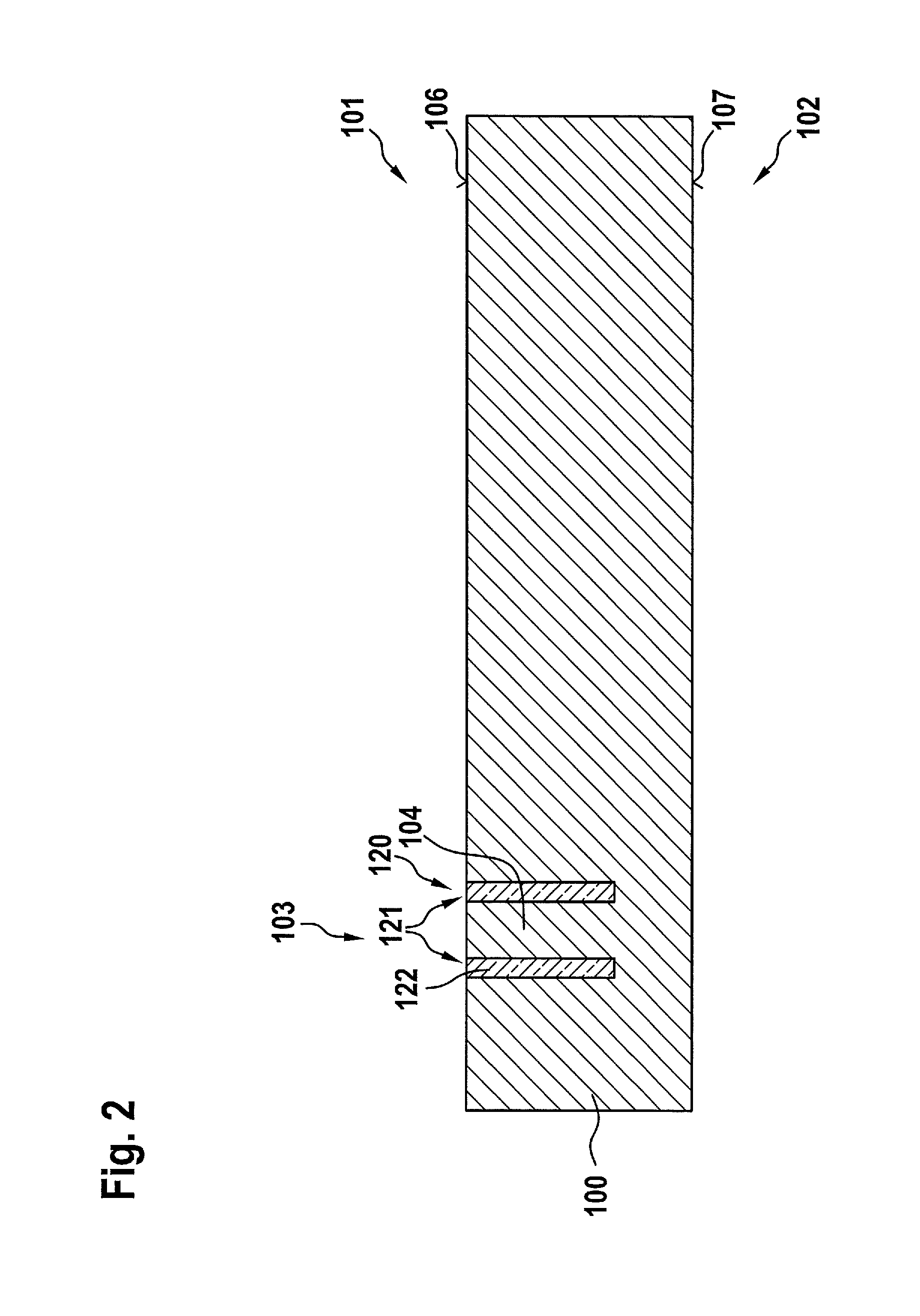
[0034]The method according to the present invention is explained in greater detail below as an example, with reference to the manufacture of a component having at least one microelectromechanical functional structure, such as a microelectromechanical motion sensor or yaw rate sensor. The through-connection is produced in a semiconductor substrate which is used as a cap wafer for the microelectromechanical functional structure situated on the functional substrate. The starting point is a semiconductor substrate, for example in the form of a silicon wafer, in which a ring-shaped insulating structure in the form of an insulating trench filled with an insulating material is initially produced. Insulating trench 121 may be produced, for example, using a customary trench method or with the aid of a laser. FIG. 1 shows semiconductor substrate 100, having a front side 101 and a back side 102 opposite from front side 101. A ring-shaped trench structure 121 is initially produced on front side...


PUM


Abstract

A method for manufacturing a component having an electrical through-connection is described. The method includes the following steps: providing a semiconductor substrate having a front side and a back side opposite from the front side, producing an insulating trench, which annularly surrounds a contact area, on the front side of the semiconductor substrate, filling the insulating trench with an insulating material, producing an electrical contact structure on the front side of the semiconductor substrate by depositing an electrically conductive material in the contact area, removing the semiconductor material remaining in the contact area on the back side of the semiconductor substrate in order to produce a contact hole which opens up the bottom side of the contact structure, and depositing a metallic material in the contact hole in order to electrically connect the electrical contact structure to the back side of the semiconductor substrate.

Description

FIELD OF THE INVENTION[0001]The present invention relates to a method for manufacturing a component, in particular a microelectromechanical component, having an electrical through-connection.BACKGROUND INFORMATION[0002]Electrical contact structures which extend through a semiconductor substrate are used, among other things, in microelectromechanical system components (MEMS, microelectromechanical system). Thus, such contact structures, also referred to as a through contact, through-connection, via (vertical interconnect access), or, in the case of a silicon substrate, as a through silicon via (TSV), are used, for example, to electrically connect various planes of the component to one another. These vertical through-connections allow a particularly space-saving design. In addition to simple rewirings, such through-connections allow individual components to be stacked on top of one another to form a so-called 3D package. Thus, for example, a sensor chip, a sensor cap, and an evaluatio...

Claims


Application Information

Patent Timeline
IPC IPC(8): H01L23/48H01L21/762
CPCH01L21/76224H01L23/481H01L24/02H01L24/29H01L24/32H01L24/83H01L24/92H01L24/94H01L2224/05009H01L2224/29111H01L2224/29124H01L2224/29147H01L2224/32145H01L2224/32225H01L2224/83193H01L2224/83805H01L2224/92H01L2224/9202H01L2224/94H01L2224/02311H01L2224/29117B81B7/007B81C1/00095B81B2207/096H01L2924/1461H01L21/76898H01L2924/351H01L2924/12042H01L2224/0231H01L2224/83H01L21/78H01L2924/00014H01L2924/01032H01L2924/00
Inventor REINMUTH, JOCHENFREY, JENSBERGMANN, YVONNE
Owner ROBERT BOSCH GMBH
Why Eureka
Try Eureka