Display device

a display device and display technology, applied in the field of display devices, can solve problems such as failure of electrical connection, and achieve the effect of preventing the deflection of an integrated circuit chip and preventing the occurrence of electrical connection failur

Inactive Publication Date: 2014-01-30
JAPAN DISPLAY INC
View PDF1 Cites 13 Cited by
  • Summary
  • Abstract
  • Description
  • Claims
  • Application Information

AI Technical Summary

Benefits of technology

[0007]It is an object of the invention to provide a display device where the occurrence of elec...

Problems solved by technology

When the center of the integrated circuit chip is deflected, all of the back surface is curved thu...

Method used


Image

  • Display device
  • Display device
  • Display device

Examples


Embodiment Construction

[0026]Hereinafter, a display device according to an embodiment of the invention is explained in conjunction with drawings.

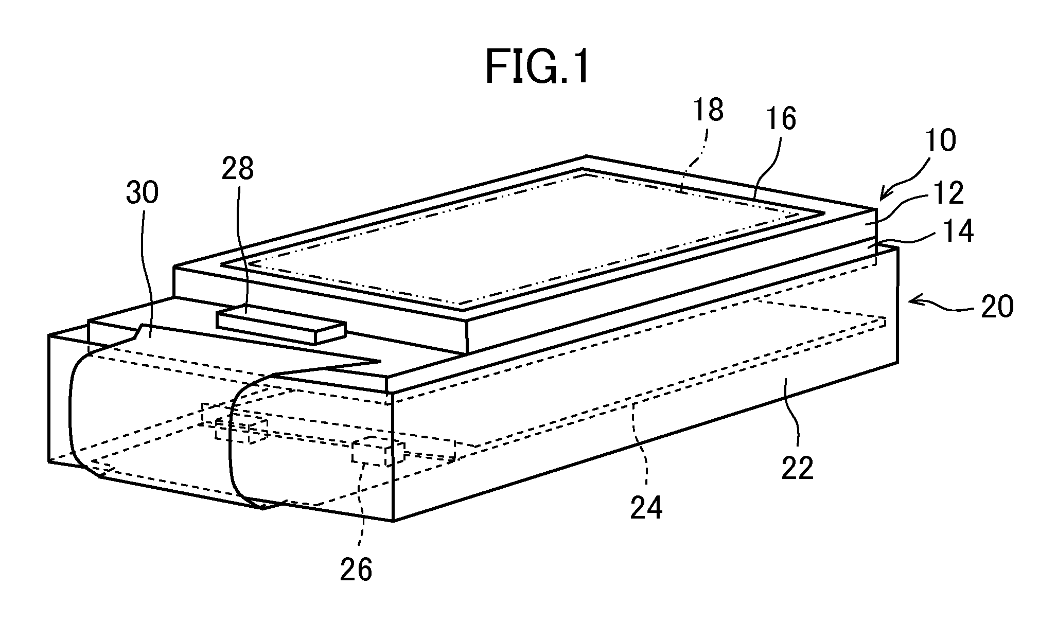
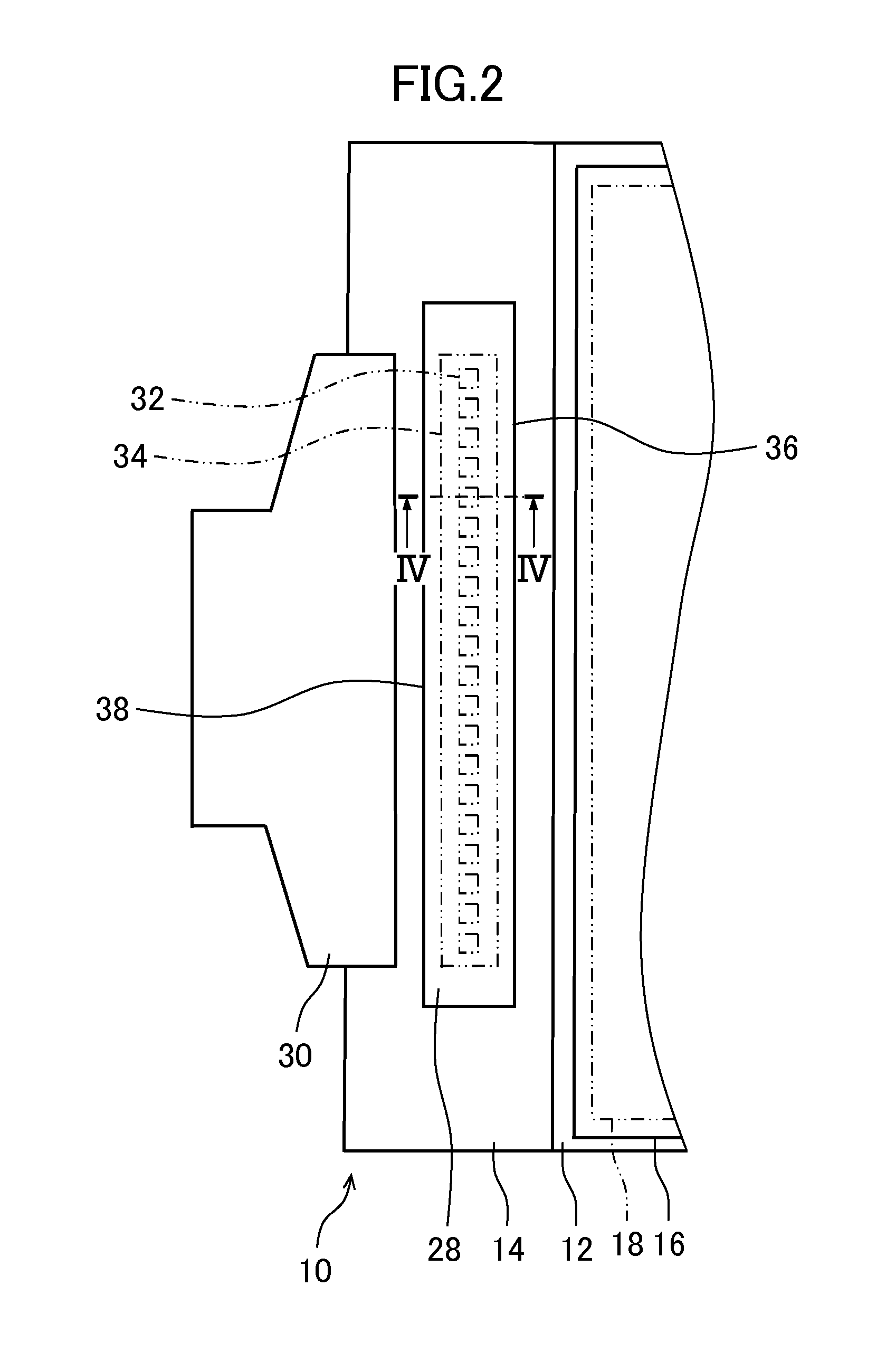
[0027]FIG. 1 is a perspective view showing the schematic constitution of the display device according to the embodiment of the invention. Although the embodiment where the invention is applied to a liquid crystal display device is explained hereinafter, the invention is also applicable to display devices other than the liquid crystal display device (for example, an EL (Electro Luminescence) display device).

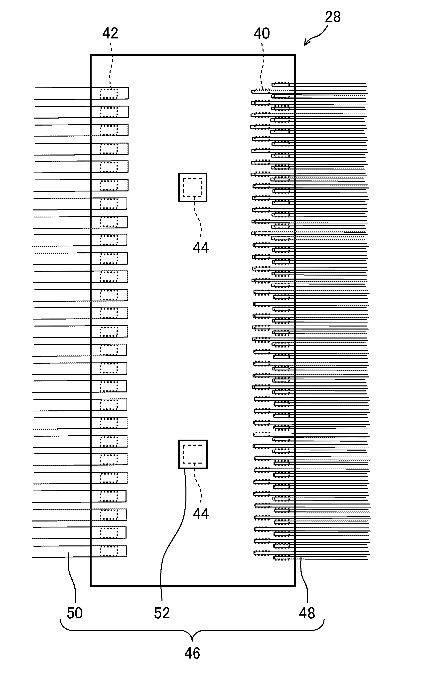
[0028]The liquid crystal display device includes a liquid crystal display panel 10 which is one example of a display panel. The liquid crystal display panel 10 includes a first substrate 12 and a second substrate 14 which are made to overlap with each other. The first substrate 12 and the second substrate 14 are respectively made of a light transmissive substrate made of glass or the like, and liquid crystal not shown in the drawing is interposed between both s...


PUM


Abstract

An integrated circuit chip includes first and second electrode terminals electrically connected to an internal circuit, and a dummy bump arranged between the first and second electrode terminals on a back surface thereof. A wiring pattern includes first lines electrically connected to the first electrode terminals below the back surface of the integrated circuit chip and extend in the direction toward a display region outside the integrated circuit chip, and second lines electrically connected to the second electrode terminals below the back surface of the integrated circuit chip and extend in the direction opposite to the display region outside the integrated circuit chip. The dummy bump is configured to avoid at least one of the electrical connection between the dummy bump and all of the first lines and all of the second lines and the electrical connection between the dummy bump and the internal circuit.

Description

CROSS-REFERENCE TO RELATED APPLICATION[0001]The present application claims priority from Japanese application JP2012-164903 filed on Jul. 25, 2012, the content of which is hereby incorporated by reference into this application.BACKGROUND OF THE INVENTION[0002]1. Field of the Invention[0003]The present invention relates to a display device.[0004]2. Description of the Related Art[0005]There has been known a technique where an integrated circuit chip which incorporates a driver therein is mounted on a liquid crystal display panel (Japanese Patent No. 3824845). There has been also known a technique where an anisotropic conductive film is used in mounting an integrated circuit chip. In a mounting process, the integrated circuit chip is heated and pressed by way of the anisotropic conductive film.[0006]Electrodes are arranged on edge portions of a back surface of the integrated circuit chip along two sides arranged opposite to each other, and a bump is provided to each electrode. However,...

Claims


Application Information

Patent Timeline
IPC IPC(8): H05K1/11
CPCH05K1/111G02F1/13454G02F1/13458H01L2224/16225H01L2224/32225H01L2224/73204H01L2924/00
Inventor ABE, HIDEAKINAKANO, YASUSHIKAWAGUCHI, HITOSHI
Owner JAPAN DISPLAY INC
Why Eureka
Try Eureka