
Single-chip push-pull bridge-type magnetic field sensor

a push-pull bridge and magnetic field sensor technology, applied in the field of single-chip push-pull bridge magnetic field sensor, can solve the problems of affecting the deposition of the first film, affecting the overall performance of the sensor, and not being ideal for manufacturing

Active Publication Date: 2014-02-06
MULTIDIMENSION TECH CO LTD
View PDF12 Cites 43 Cited by
  • Summary
  • Abstract
  • Description
  • Claims
  • Application Information

AI Technical Summary

Benefits of technology

The present invention is about a way to make sensors that measure magnetic fields using a special design and production process. These sensors have multiple arms, each containing special elements that change resistance when exposed to magnetic fields. The sensors are arranged in a way that they can detect changes in magnetic fields along a specific axis. The sensors use special magnets to bias the resistance elements, which makes them very sensitive to small changes in magnetic fields. The invention introduces a new method for making these sensors that allows for the efficient production of large numbers of them.

Problems solved by technology

It is common to use a push-pull sensor bridge rather than a single sensor element in order to produce a magnetic field sensor, since bridge sensors have higher sensitivity, and because a bridge configuration removes offset and suppresses thermal effects magnetoresistive This however is not ideal for manufacturing, since there are no standard methods for setting the magnetization direction of the adjacent arms.
This method is complex production process, depending on the specific nature of the films, if a second anneal is needed; it can significantly affect the deposition of the first film.
Because two separate deposition steps are used, it is difficult to match the resistance and performance of bridge legs built form the different films, degrading the overall performance of the sensor;
However, because of the multi-chip packaging technology there are performance and cost disadvantages.
The package size large; production costs are high; alignment is difficult and it is not always possible to achieve an accurate 180° flip; If the sensor chips are not properly aligned at 180°, then the performance characteristics of the two chips may not match well.
In short, although the Multi-Chip Packaging process is standard and capable of producing good push-pull sensor bridges, it brings about cost and potential performance problems;
(3) Laser Assisted Local Magnetic Annealing: In this method, GMR or MTJ wafers are initially annealed at high temperature in a strong magnetic field, which sets the magnetization of the different bridge arms in the same direction. At a later step in the process, a scanning laser beam plus reversed magnetic field is used to locally heat the wafer in the regions where the pinned layer needs to be reversed. Although it sounds easy in concept, the local laser heating method requires special equipment that is not commercially available, and development of the equipment is expensive. The process is expensive to utilize, since it requires a long time to process an entire wafer. Performance is also an issue, since it can be difficult to properly match other performance of the push and pull sensor arms that result in the process, and the consistency of the different bridge arms cannot be guaranteed.

Method used


Image

  • Single-chip push-pull bridge-type magnetic field sensor
  • Single-chip push-pull bridge-type magnetic field sensor
  • Single-chip push-pull bridge-type magnetic field sensor

Examples


Embodiment Construction

[0031]With reference to FIGS. 1-13 below, preferred embodiments of the present invention will be described in detail so that the advantages and features of the present invention can be more easily understood by a person skilled in the art, and thus more clearly defining the scope of protection of the present invention.

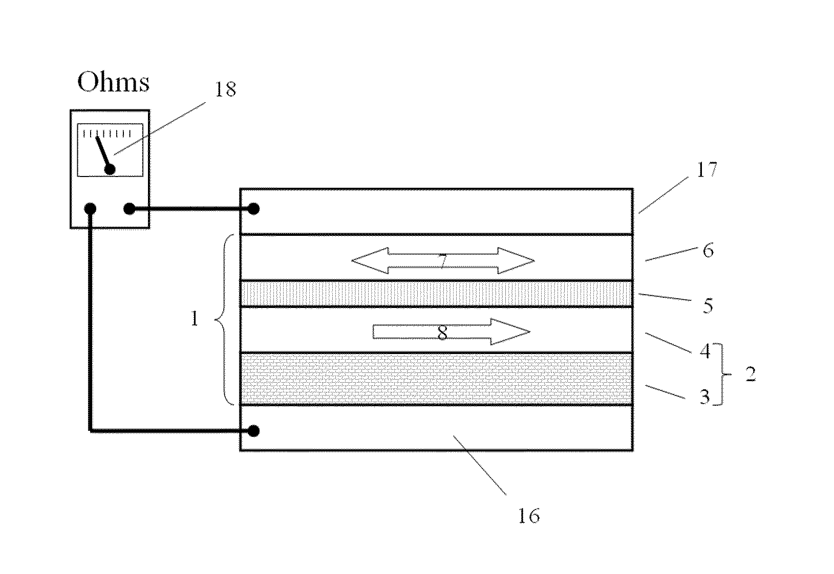
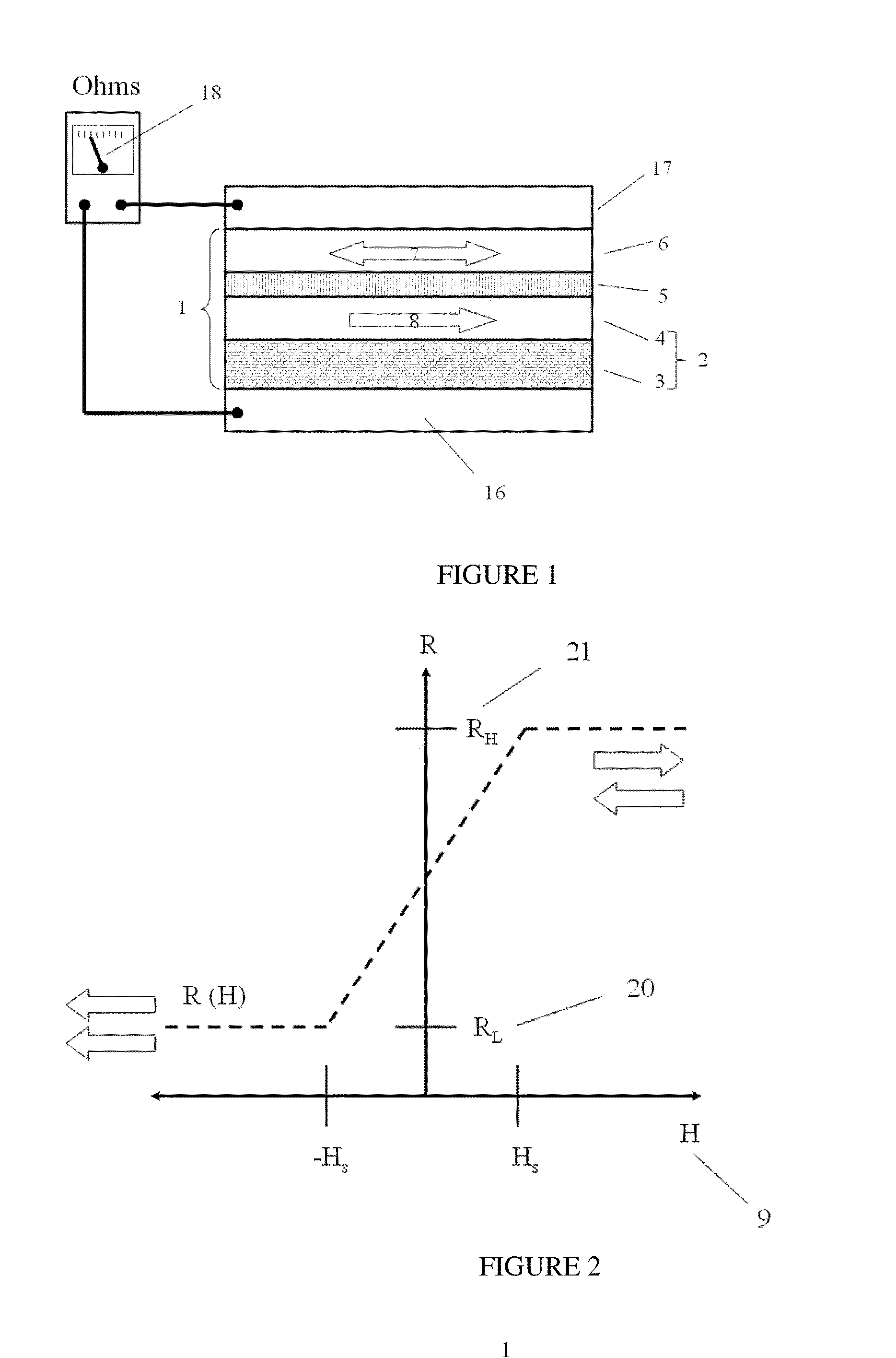
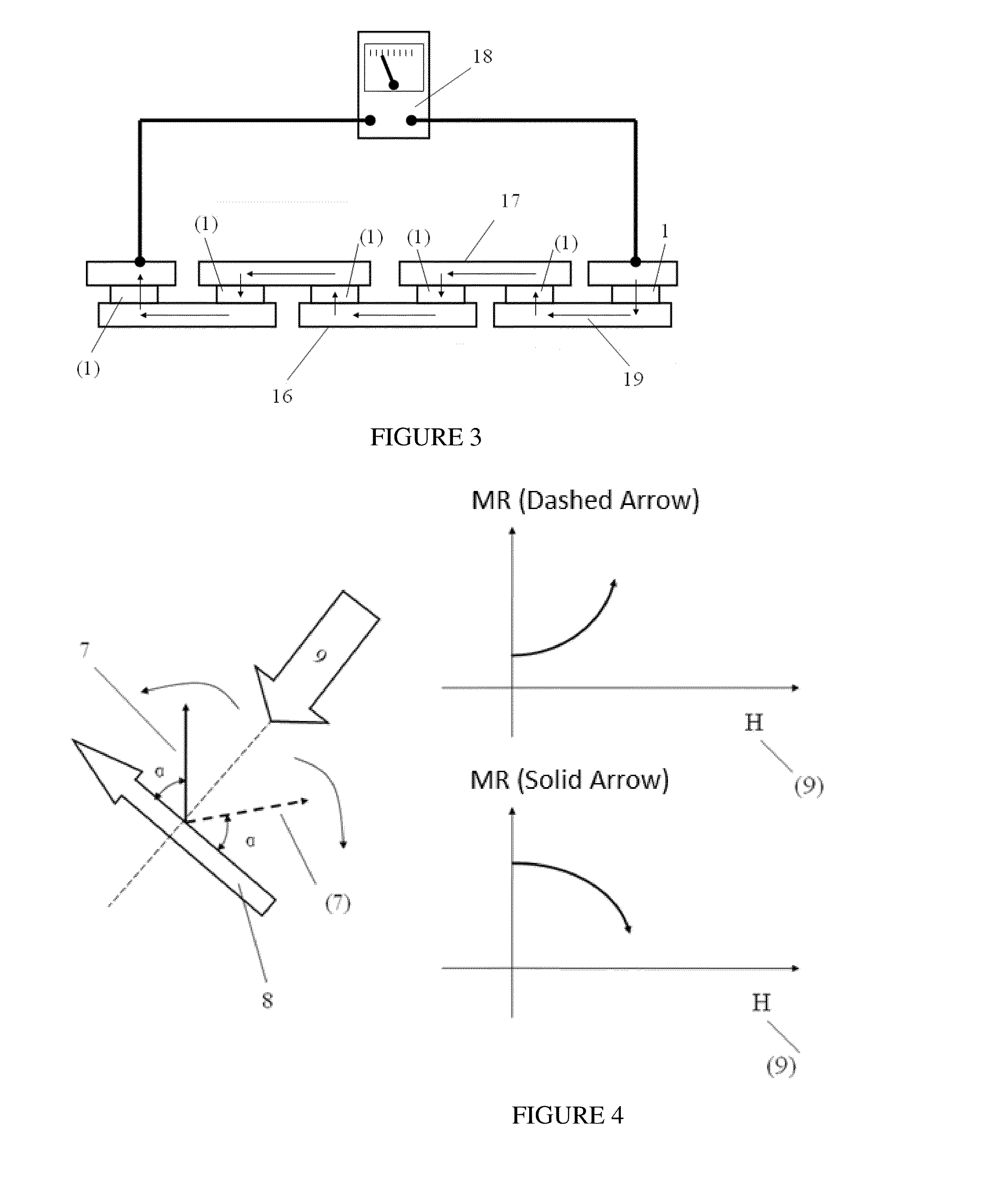
[0032]FIG. 1 illustrates a standard MTJ element. A standard MTJ element 1 comprises a magnetic free layer 6 and a magnetic pinned layer 2, which are separated by a tunnel barrier layer 5. The free layer 6 is made from a ferromagnetic material, and the magnetization direction of the magnetic free layer 7 can change in response to a change of the external magnetic field. The pinned layer 2 magnetization direction does not change, and it is set into direction 8. A magnetic pinned layer is often comprised of antiferromagnetic layer 3 above or below a ferromagnetic layer 4. The MTJ structure is usually deposited on the conductive seed layer 16 and it is capped with an elect...


PUM


Abstract

The present invention discloses a design of a single-chip push-pull bridge sensor, composed of magnetoresistive elements, utilizing on-chip permanent magnets. The permanent magnets are oriented to preset magnetization directions of free layers of adjacent sensor bridge arms so that they point to different directions with respect the same sensing direction, enabling push-pull operation. The push-pull bridge sensor of the present invention is integrated on a single chip. Additionally, an on-chip coil is disclosed to reset or calibrate the magnetization directions of the free layers of the magnetoresistive elements.

Description

CROSS-REFERENCE TO A RELATED APPLICATION[0001]This application is a 35 U.S.C. §371 national phase application of PCT / CN2012 / 073495, filed on Apr. 1, 2012, which claims priority to a Chinese Patent Application No. CN 201120097042, filed on Apr. 16, 2011, and a Chinese Patent Application No. CN201110326725, filed on Oct. 25, 2011, incorporated herein by reference in its entirety.TECHNICAL FIELD[0002]The invention relates to a magnetic field sensors, in particular single-chip push-pull magnetic field sensor bridges.BACKGROUND ART[0003]Magnetic field sensors can be used to detect magnetic field direction, intensity, and the location of magnetic objects. Magnetoresistive sensors can be used to produce a high performance push-pull sensor bridge with the advantages of low offset, high sensitivity, and good temperature stability. Magnetic tunnel junction (MTJ) sensors are a new type of magnetorestive sensor which has been used recently in various applications It utilizes a magnetic multilay...

Claims


Application Information

Patent Timeline
Patent Type & Authority Applications(United States)
IPC IPC(8): G01R33/09H10N50/10H10N50/80
CPCG01R33/09G01R33/098G01D5/145G01R33/0005G01R33/0011G06Q2220/00G06Q10/00H04L9/50H10B61/00H10N59/00H10N50/10G07F1/00
Inventor JIN, INSIKLEI, XIAOFENGDEAK, JAMES GEZASHEN, WEIFENGXUE, SONGSHENGLI, WEI
Owner MULTIDIMENSION TECH CO LTD
Learn More