
Memory channel that supports near memory and far memory access

a memory channel and memory technology, applied in the field of computer systems, can solve the problems of data loss, power consumption of dram-based memory, and limiting factors of computer innovation today, and achieve the effects of reducing the cost of memory and storage technology, reducing the cost of memory and storage, and improving the efficiency of memory and storag

Active Publication Date: 2014-02-06
TAHOE RES LTD
View PDF7 Cites 120 Cited by
  • Summary
  • Abstract
  • Description
  • Claims
  • Application Information

AI Technical Summary

Benefits of technology

The invention relates to a computer system with improved memory and storage configurations. The technical effects of the invention include a multi-level memory hierarchy with a non-volatile memory tier, a cache management protocol, and a memory and storage hierarchy that reduces power consumption and improves performance. The invention also utilizes phase-change memory, which provides higher performance and faster switching times compared to flash memory. The invention can be implemented in computer systems and can improve the speed and efficiency of the computer system.

Problems solved by technology

One of the limiting factors for computer innovation today is memory and storage technology.
DRAM-based memory consumes power even when no memory reads or writes occur because it must constantly recharge internal capacitors.
DRAM-based memory is volatile, which means data stored in DRAM memory is lost once the power is removed.
These I / O adapters and I / O protocols consume a significant amount of power and can have a significant impact on the die area and the form factor of the platform.
Flash memory devices that are currently available in the market generally have limited speed (e.g., 50 MHz).

Method used


Image

  • Memory channel that supports near memory and far memory access
  • Memory channel that supports near memory and far memory access
  • Memory channel that supports near memory and far memory access

Examples


Embodiment Construction

[0027]In the following description, numerous specific details such as logic implementations, opcodes, means to specify operands, resource partitioning / sharing / duplication implementations, types and interrelationships of system components, and logic partitioning / integration choices are set forth in order to provide a more thorough understanding of the present invention. It will be appreciated, however, by one skilled in the art that the invention may be practiced without such specific details. In other instances, control structures, gate level circuits and full software instruction sequences have not been shown in detail in order not to obscure the invention. Those of ordinary skill in the art, with the included descriptions, will be able to implement appropriate functionality without undue experimentation.

[0028]References in the specification to “one embodiment,”“an embodiment,”“an example embodiment,” etc., indicate that the embodiment described may include a particular feature, st...


PUM


Abstract

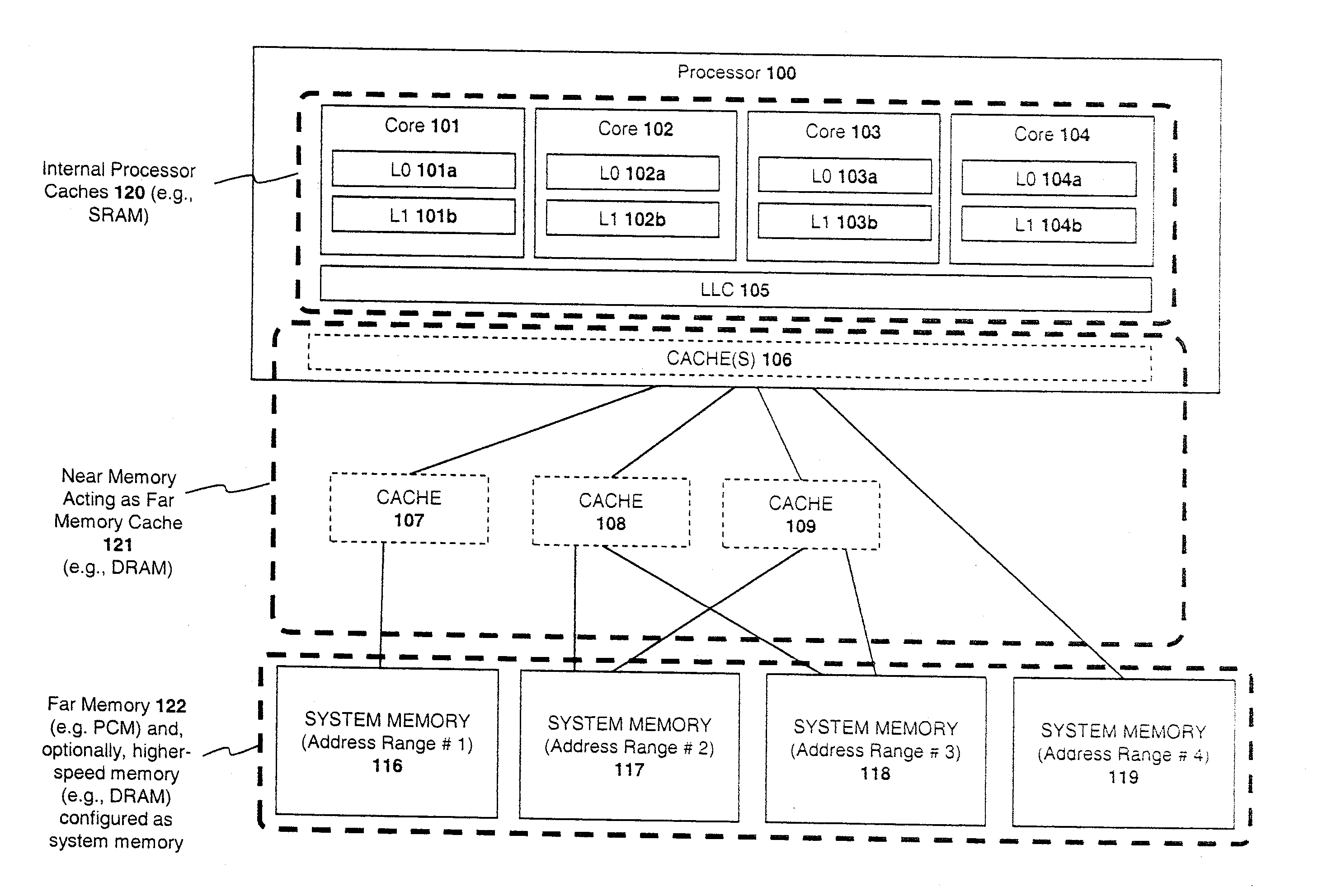
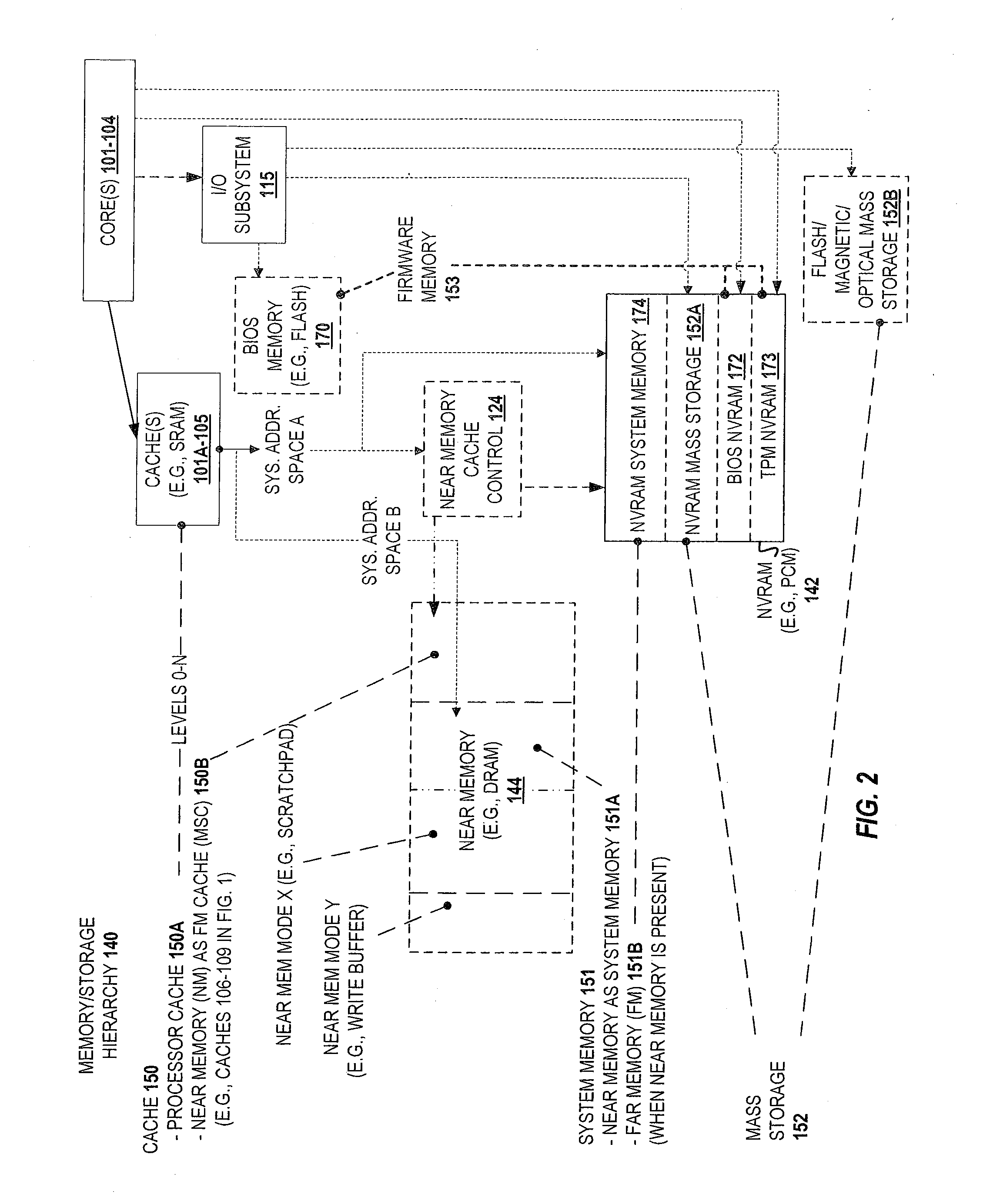
A semiconductor chip comprising memory controller circuitry having interface circuitry to couple to a memory channel. The memory controller includes first logic circuitry to implement a first memory channel protocol on the memory channel. The first memory channel protocol is specific to a first volatile system memory technology. The interface also includes second logic circuitry to implement a second memory channel protocol on the memory channel. The second memory channel protocol is specific to a second non volatile system memory technology. The second memory channel protocol is a transactional protocol.

Description

BACKGROUND[0001]1. Field of the Invention[0002]This invention relates generally to the field of computer systems. More particularly, the invention relates to an apparatus and method for implementing a multi-level memory hierarchy including a non-volatile memory tier.[0003]2. Description of the Related Art[0004]A. Current Memory and Storage Configurations[0005]One of the limiting factors for computer innovation today is memory and storage technology. In conventional computer systems, system memory (also known as main memory, primary memory, executable memory) is typically implemented by dynamic random access memory (DRAM). DRAM-based memory consumes power even when no memory reads or writes occur because it must constantly recharge internal capacitors. DRAM-based memory is volatile, which means data stored in DRAM memory is lost once the power is removed. Conventional computer systems also rely on multiple levels of caching to improve performance. A cache is a high speed memory posit...

Claims


Application Information

Patent Timeline
IPC IPC(8): G06F12/08
CPCG06F12/0802G06F9/467G06F11/1064G06F12/0804G06F12/0868G06F12/0897G06F13/1668G06F13/1694G06F13/4068G06F13/42G06F2212/2024G06F2212/1016G06F2212/1044G06F12/0238G06F12/0811G06F13/4234G06F2212/1008G06F2212/7203Y02D10/00
Inventor NALE, BILLRAMANUJAN, RAJ K.SWAMINATAN, MUTHUKUMAR P.THOMAS, TESSILPOLEPEDDI, TAARINYA
Owner TAHOE RES LTD
Learn More