Method of manufacturing a semiconductor device

Inactive Publication Date: 2014-02-13
SK HYNIX INC
View PDF4 Cites 4 Cited by
  • Summary
  • Abstract
  • Description
  • Claims
  • Application Information

AI Technical Summary

Benefits of technology

[0007]Accordingly, a need arises for a simplified manufacturing process for semiconductor devices having patterns with different widths. When spacer patterning technology is employed, a width of a word line is defined by a width of a spacer. Spacers are formed through a series of processes, including forming a sacrificial pattern on an etch target layer, forming a spacer layer over a surface of the sacrificial pattern, etching the spacer layer to expose the sacrificial pattern with the spacer layer remaining along a sidewall of the sacrificial pattern, and removing the exposed

Problems solved by technology

However, the addition of a process for forming the

Method used


Image

  • Method of manufacturing a semiconductor device
  • Method of manufacturing a semiconductor device
  • Method of manufacturing a semiconductor device

Examples


Embodiment Construction

[0014]Hereinafter, various embodiments of the present invention will be described in detail with reference to the accompanying drawings. The present invention may, however, be embodied in different forms and should not be construed as limited to the embodiments set forth herein. Although embodiments in accordance with the present invention are described with reference to a number of examples thereof, it should be understood that numerous variations and modifications can be devised by those skilled in the art that will fall within the spirit and scope of the invention. Like reference numerals refer to like elements throughout the specification and drawings.

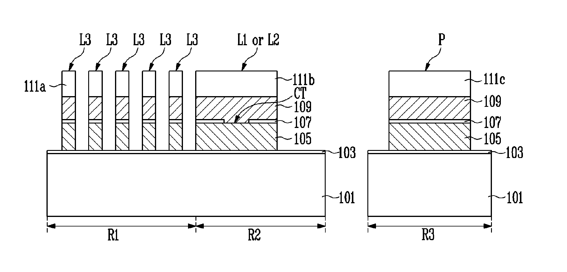
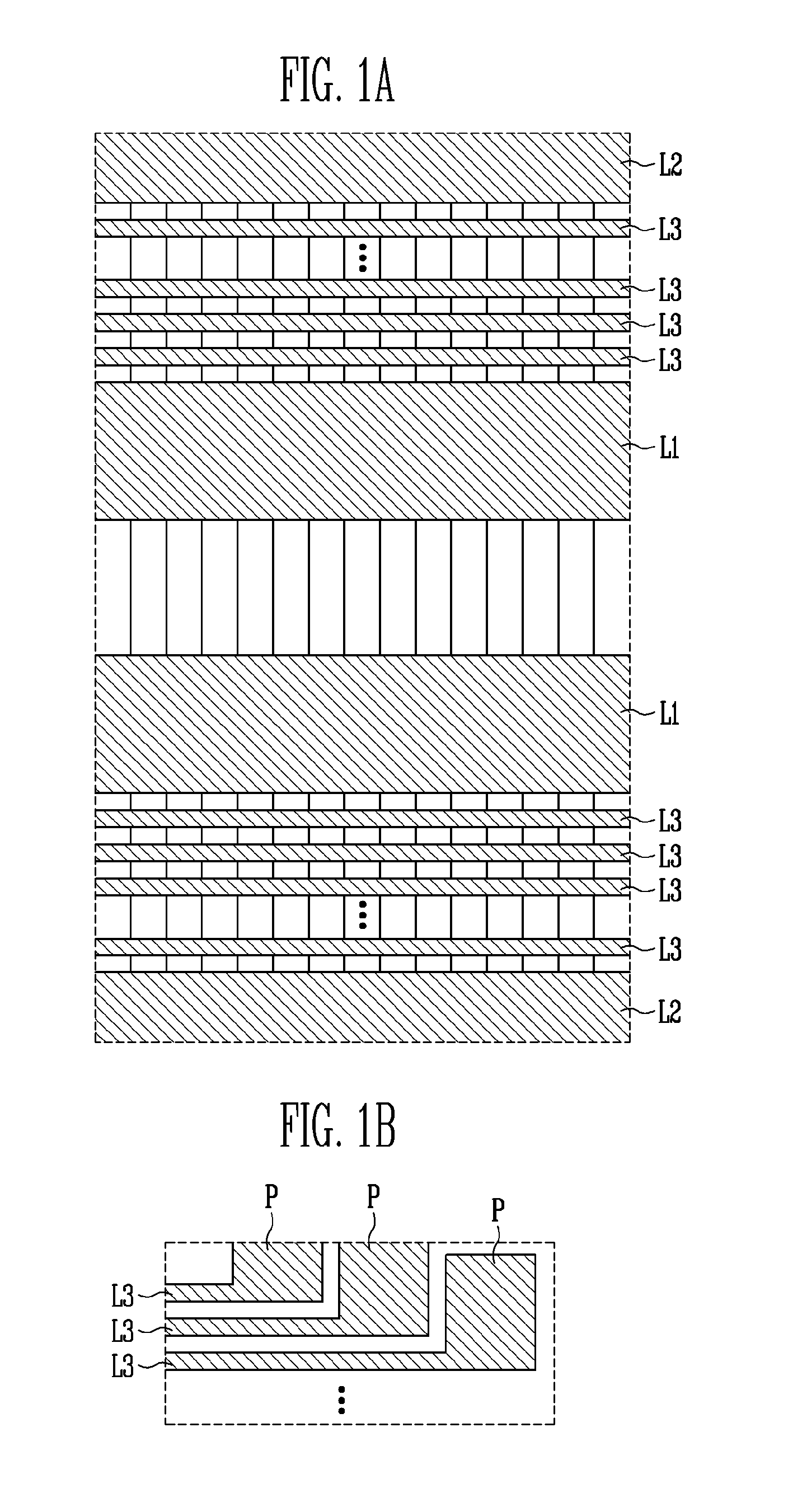
[0015]FIG. 1A illustrates a cell region where gate lines of a NAND flash memory device are formed. FIG. 1B illustrates a peripheral region where pad portions coupled to the gate lines of the NAND flash memory device are formed.

[0016]Referring now to FIG. 1A, the gate lines of the NAND flash memory device may include selection lines...


PUM


Abstract

A method of manufacturing a semiconductor device having patterns with different widths. The method includes etching a sacrificial pattern using a protective pattern that has a greater width and remains during an etch process of a spacer layer. Since the sacrificial pattern that has a greater width and remains under the protective pattern having a greater width is used as a pad mask pattern, a separate process of forming a pad mask pattern may not be necessary. Therefore, a method of manufacturing a semiconductor device may be simplified.

Description

CROSS-REFERENCE TO RELATED APPLICATION[0001]The present application claims priority to Korean patent application number 10-2012-0086896 filed on Aug. 8, 2012, in the Korean Intellectual Property Office, which is incorporated by reference herein in its entirety.BACKGROUND[0002]1. Technical Field[0003]The present invention relates generally to a method of manufacturing a semiconductor device and, more particularly, to a method of manufacturing a semiconductor device having patterns with different widths.[0004]2. Related Art[0005]Semiconductor devices may include patterns of various sizes. For example, a NAND flash memory device includes gate lines comprised of a source select line, a drain select line and a plurality of word lines interposed therebetween. In general, a word line has a smaller width than a source select line or a drain select line. The source select line is coupled to a gate of a source select transistor, the drain select line is coupled to a gate of a drain select tra...

Claims


Application Information

Patent Timeline
IPC IPC(8): H01L21/308
CPCH01L27/11529H01L21/28132H01L21/823456H01L21/28273H01L21/308H01L21/823468H01L29/40114H10B41/41H01L21/0273
Inventor PARK, CHANG, KI
Owner SK HYNIX INC
Why Eureka
Try Eureka