

Method for transferring inp film
- Summary
- Abstract
- Description
- Claims
- Application Information
AI Technical Summary
Benefits of technology
Problems solved by technology
Method used
Image

Examples
Embodiment Construction
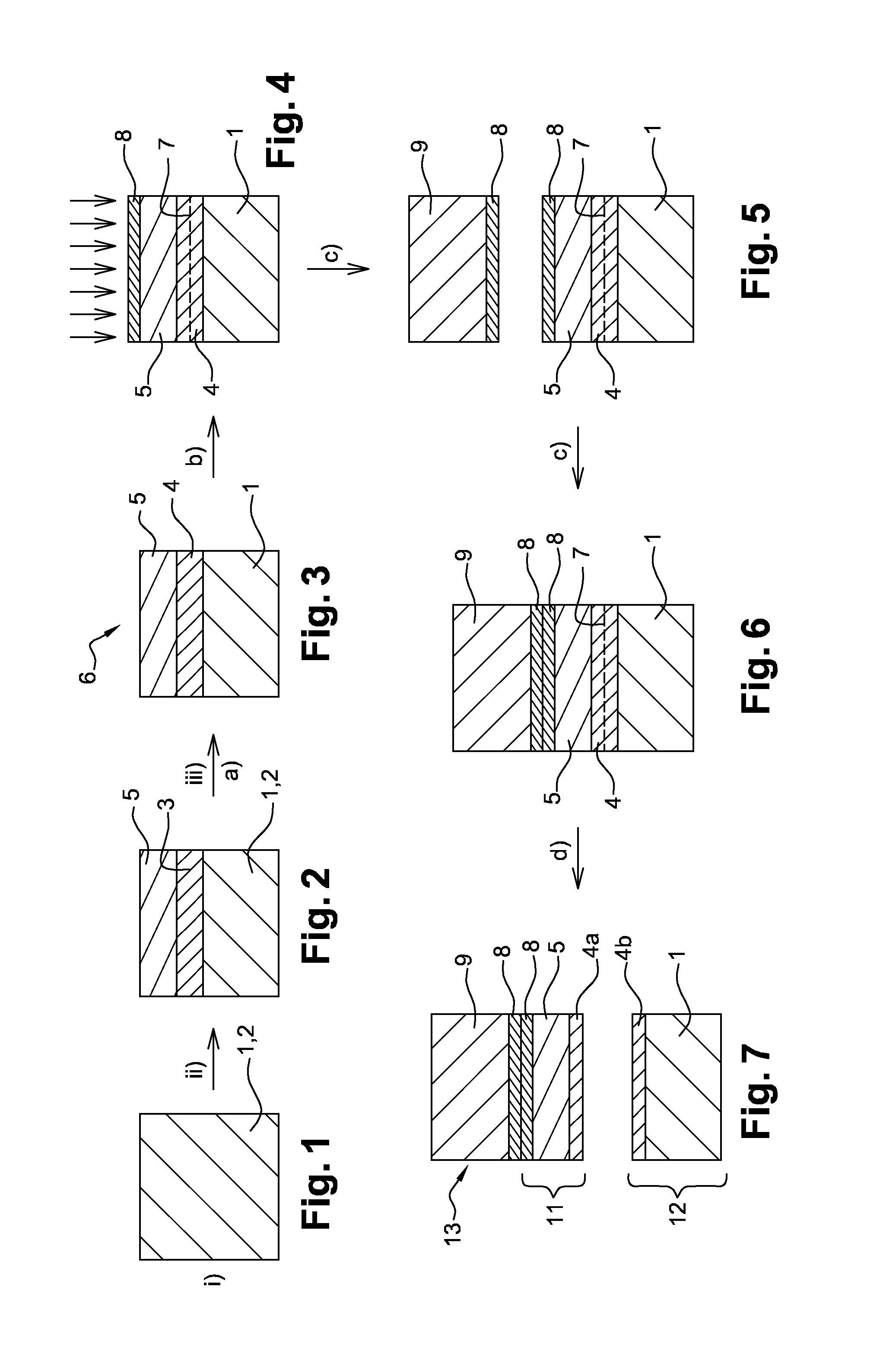
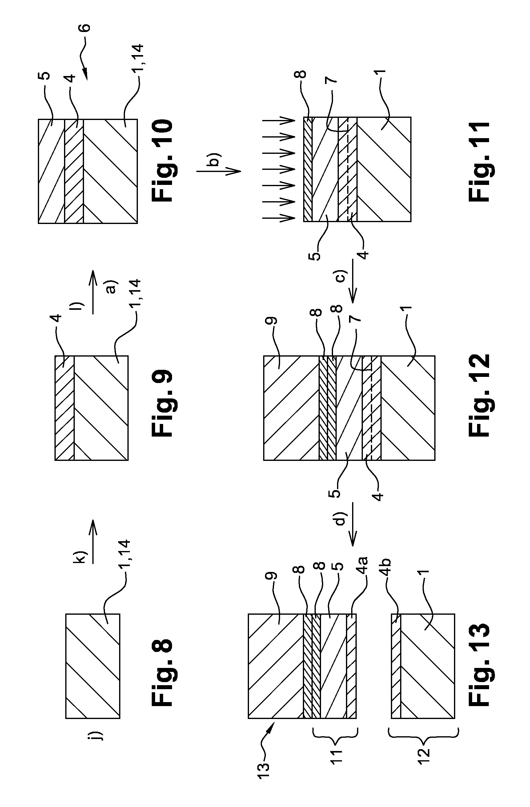
[0045]FIG. 1 illustrates a substrate 1 formed of an initial layer 2, for example in resistive InP, having a diameter of 50 mm (step i). FIG. 2 illustrates the implanting of dopant ion species e.g. Si+ ions at an energy of about 150 KeV and dose of about 5.1014 Si / cm2 so as to form a buried layer 3 implanted in the initial layer 2 (step ii). FIG. 3 illustrates the application of heat treatment by rapid thermal annealing (RTA), in the case described here, at a temperature of about 850° C. for 5 seconds, so as electrically to activate the implanted dopant species and so that the buried layer 3 becomes a doped thin layer 4 with a concentration of activated dopants ranging from 2.1018 to 3.1019 Si / cm2 depending on the implantation profile. In the case concerned here, this doped thin layer 4 lies at a depth of between 0 and 300 nm underneath the implanted surface of the substrate 1 (step iii), the surface layer 5 then forming the surface part of the doped thin layer 4 and is therefore als...
PUM
 Abstract
Description
Claims
Application Information