
Textured imaging member
- Summary
- Abstract
- Description
- Claims
- Application Information
AI Technical Summary
Benefits of technology
Problems solved by technology
Method used
Image

Examples
example 1
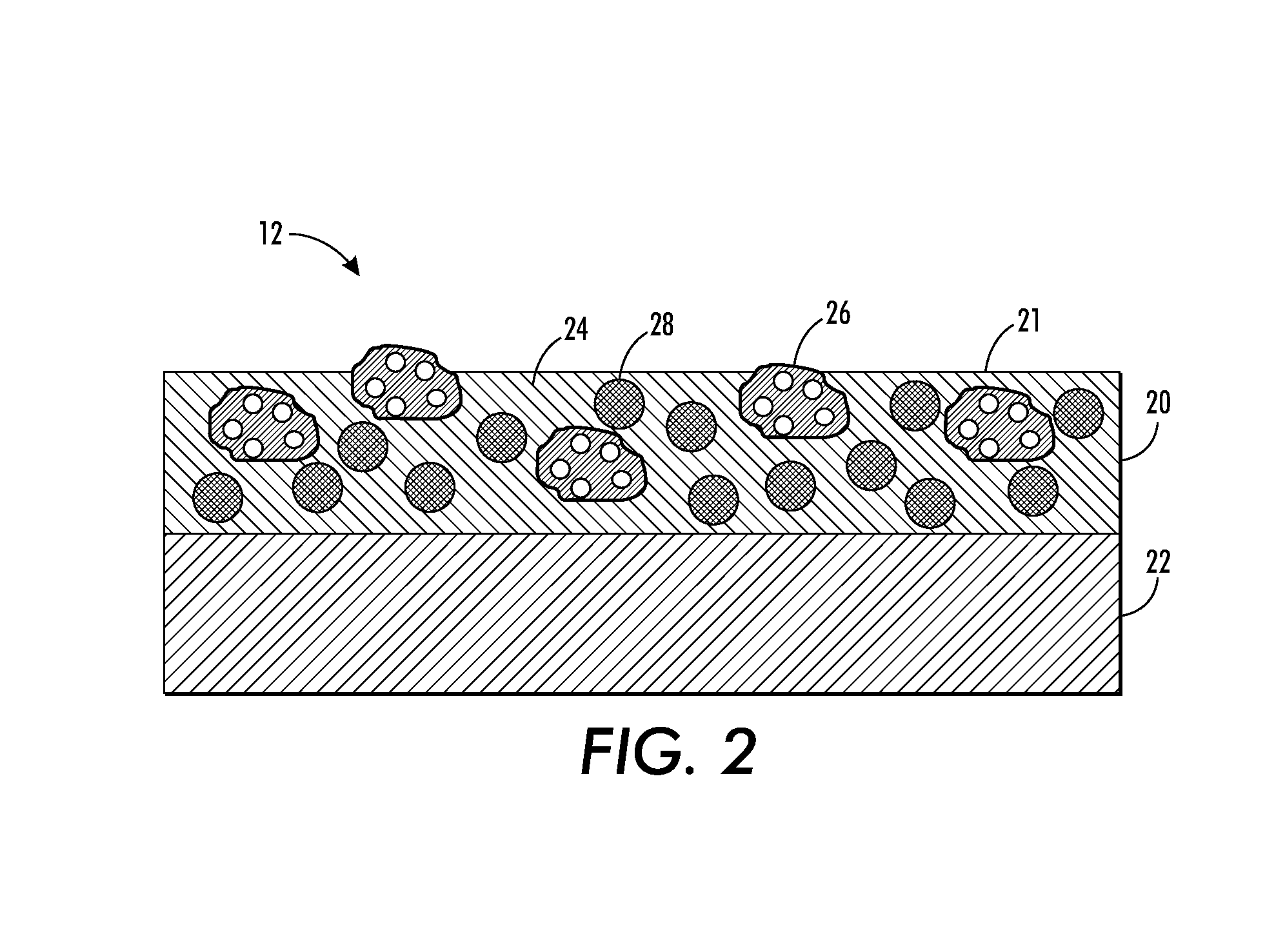
[0126]In Example 1, the surface layer comprised silicone, 3 wt % silica aerogel, and 10 wt % carbon black. The silica aerogel had an average particle size of about 10 μm. FIGS. 3A-C are SEM images from a top, orthogonal view, a top 45° view, and a cross-sectional view, respectively. The SEM images show that the roughness produced at the surface is approximately on a 10 μm scale, which was the same as the average particle size of the aerogel component. The submicron-sized carbon black particles can be observed as being dispersed between the silica aerogel particles in FIG. 3C.
[0127]Test surfaces containing silica aerogel were matte in appearance versus control samples lacking an aerogel component that were shiny in appearance. The surfaces with and without aerogel were smooth and level. The aerogel test surface layers exhibited higher cohesion and strength when stretched and were less prone to tearing. The addition of silica aerogel particles to silicone resulted in an increase in te...
example 2
[0128]In Example 2, the surface layer comprised silicone and 3 wt % silica aerogel. The silica aerogel had a mean particle size of 10 μm and was not milled. FIG. 4A is a SEM of the surface layer.
example 3
[0129]In Example 3, the procedure of Example 2 was followed except that the silica aerogel particles were milled in toluene for about 0.5 hours. Milling was performed for about 0.5 hours in toluene to achieve a mean particle size of about 2.5 μm. The milled particles had a mean particle size of about 2.5 μm. FIG. 4B is a SEM of the surface layer. SEM imaging of the surface indicated a particle size range which included larger particles. These larger particles could have been removed by sieving.
PUM
 Abstract
Description
Claims
Application Information