Copper reflow process

a technology of copper reflow and copper, which is applied in the direction of semiconductor/solid-state device manufacturing, basic electric elements, electric apparatus, etc., can solve the problems of aluminum resistance becoming non-negligible, resistance-capacitance (rc) time delay of the circuit, and the deficiency of aluminum and its allows becoming limiting factors in achieving superior performance. , to achieve the effect of improving the adhesion, reducing variability, and better modeling a process

Inactive Publication Date: 2003-07-24
INTEL CORP
View PDF0 Cites 17 Cited by
  • Summary
  • Abstract
  • Description
  • Claims
  • Application Information

AI Technical Summary

Benefits of technology

0044] FIG. 2e shows the cross section of FIG. 2d after the completion of an etch back process step. In a preferred embodiment of the present invention, well known chemical-mechanical polishing processes can be used to etch the conductive layer 203 from the upper surfaces of dielectric layer 200. Thus, the portion of the conductive layer 203 which exists substantially outside the groove 202 is removed thereby isolating conductive layer 203 to the groove 202. In a preferred embodiment of the present invention, an upper portion of dielectric layer 200 is also removed as part of an over-etch process to be sure most of the conductive layer 203 which resides substantially outside the groove 202 has been removed. In an alternate embodiment of the present invention, an alternate etch process such as wet chemical etch, RE, back sputter, ion mill, or mechanical polishing can be used to remove the portion of the conductive layer 203 which resides substantially outside the groove 202. Note that etching techniques such as polishing additionally serve to planarize the surface of the substrate.
0045] FIGS. 3a-3e illustrate a more detailed description of a preferred embodiment of the present invention already shown in FIGS. 2a-2e in which a barrier layer is specifically illustrated as part of the conductive layer. FIG. 3a is analogous to FIG. 2b and displays a portion of substrate 306 above which dielectric layers 300 and 301 have been formed. Dielectric layer 300 has been etched, selectively grown, or selectively deposited in order to create the recessed region or groove 302 therein. See the discussion above for a more detailed description of an embodiment by which the substrate of FIG. 3a may be formed and suggested materials of which it may be constructed.
0046] FIG. 3b shows the same region displayed in FIG. 3a after a barrier layer 303 has been formed. This barrier layer may serve one or more of several functions. For example, the barrier layer may be used to improve the adhesion between a subsequently formed layer and another layer. This helps prevent, for example, delamination or peeling from occurring during processing. Delamination may cause significant yield or reliability problems. The barrier layer may additionally serve to, for example, prevent materials contained within a subsequently formed layer from contaminating other regions of the semiconductor device, provide a more uniform layer onto which a subsequent layer may be formed in order to better model a process and reduce variability, improve the electrical contact between a subsequently formed conductive layer and another conductive layer, improve the wetting and agglomeration characteristics of a subsequently formed layer, prevent substrate damage by shielding against the radiation used for reflow, or passivate an underlying or subsequently formed layer.
0047] Note that in accordance with this embodiment of the present invention, barrier layer 303 displayed in FIG. 3b has been deposited along the walls of groove 302 (conformal coverage). In an alternate embodiment of the present invention, barrier layer 303 may be deposited at the bottom of groove 302 and at the upper surfaces of dielectric layer 300 but not substantially along the walls of groove 302. Barrier layers constructed out of one or more of the following materials may exhibit one or more of the desired properties stated above: oxide, nitride, silicon oxynitride, silicon carbide. Mo, MoN, Ta, TaN, W, WN, V, VN, Nb, NbN, Ti, and TiN.

Problems solved by technology

While aluminum has very attractive features for use as an electrical interconnection, such as low electrical resistivity and strong adhesion to silicon dioxide (SiO.sub.2), as VLSI dimensions reach into the deep-submicron Ultra Large Scale Integration (ULSI) regime, the deficiencies of aluminum and its allows become limiting factors in achieving superior performance.
For example, as the width of electrical interconnections becomes narrower, the resistance of aluminum becomes non-negligible and begins to contribute significantly to the resistance-capacitance (RC) time delay of the circuit.
Additionally, with decreasing dimensions, design rules become increasingly restricted by aluminum interconnection reliability concerns such as electromigration, stress-induced void formation, hillock suppression, and current density limitations.
One of the main reasons why the use of Cu and its alloys for interconnection applications has not been more widespread is because a manufacturable dry-etch process has not yet been demonstrated that can pattern Cu-based materials using standard photolithographic techniques.
An inadequately filled recessed region in a damascene process flow leads to the creation of a void or tunnel.
If the top surface of the substrate is etched back at this point, gap 104 will remain inside groove 102 leading to the problems described below as well as limiting the current carrying capability of the electrical interconnection.
Gaps and voids can cause significant problems in a semiconductor manufacturing process and are considerable issues for sputtered and evaporated films.
One problem with gaps and voids is that they can trap impurities which can harm the semiconductor device in subsequent process steps.
These trapped etchant chemicals may then contaminate the semiconductor device which could degrade reliability.
Trapped etchant chemicals may also continue to etch the electrical interconnection 103 resulting in the thinning of electrical interconnection 103 or the creation of a electrical open, thereby resulting in a failure.
Interconnection thinning may lead to reliability problems such as electromigration and current-carrying limitations.
Additionally, trapped contaminants may expand upon subjecting the semiconductor substrate to subsequent high temperature processing steps.
Such expansion could cause significant damage to adjoining surface features of the semiconductor device.
Finally, trapped contaminants may escape during, for example, a subsequent process step thereby contaminating all other semiconductor devices within the process chamber.
While such optimization techniques may be suitably employed to fill interconnections of this particular width on a semiconductor substrate, the problem is that grooves of widths for which the process has not been optimized run a much higher risk of void formation.
Such dependence degrades the manufacturability of such processes.
One reason why Cu sputtering is more desirable is that there is a significant cost associated with performing CVD of Cu.
Equipment necessary to form CVD Cu layers is currently under development and not yet readily available for high production manufacturing environments.
Additionally, the materials necessary to deposit CVD Cu layers are expensive, still under investigation, and the films are not likely to be very pure.
Therefore, CVD of Cu is expensive and considerably adds to the total manufacturing cost of a semiconductor device.
Also, it is not yet known if certain important alloys of Cu are capable of being deposited using a CVD system.
These seams may be undesirable due to, for instance, their negative impact on the grain size of the conductive layer and their susceptibility to trapping impurities.
Finally, CVD techniques which exhibit low sticking coefficients also exhibit low deposition rates.
However, these higher sticking coefficient CVD processes exhibit the same short-comings as the high sticking coefficient processes discussed above.
However, sputter deposition systems have exhibited significant limitations in their ability to fill the recessed regions in damascene process flows as discussed above.
These limitations have precluded the applicability of sputter deposition systems in a damascene process.

Method used


Image

  • Copper reflow process
  • Copper reflow process
  • Copper reflow process

Examples


Embodiment Construction

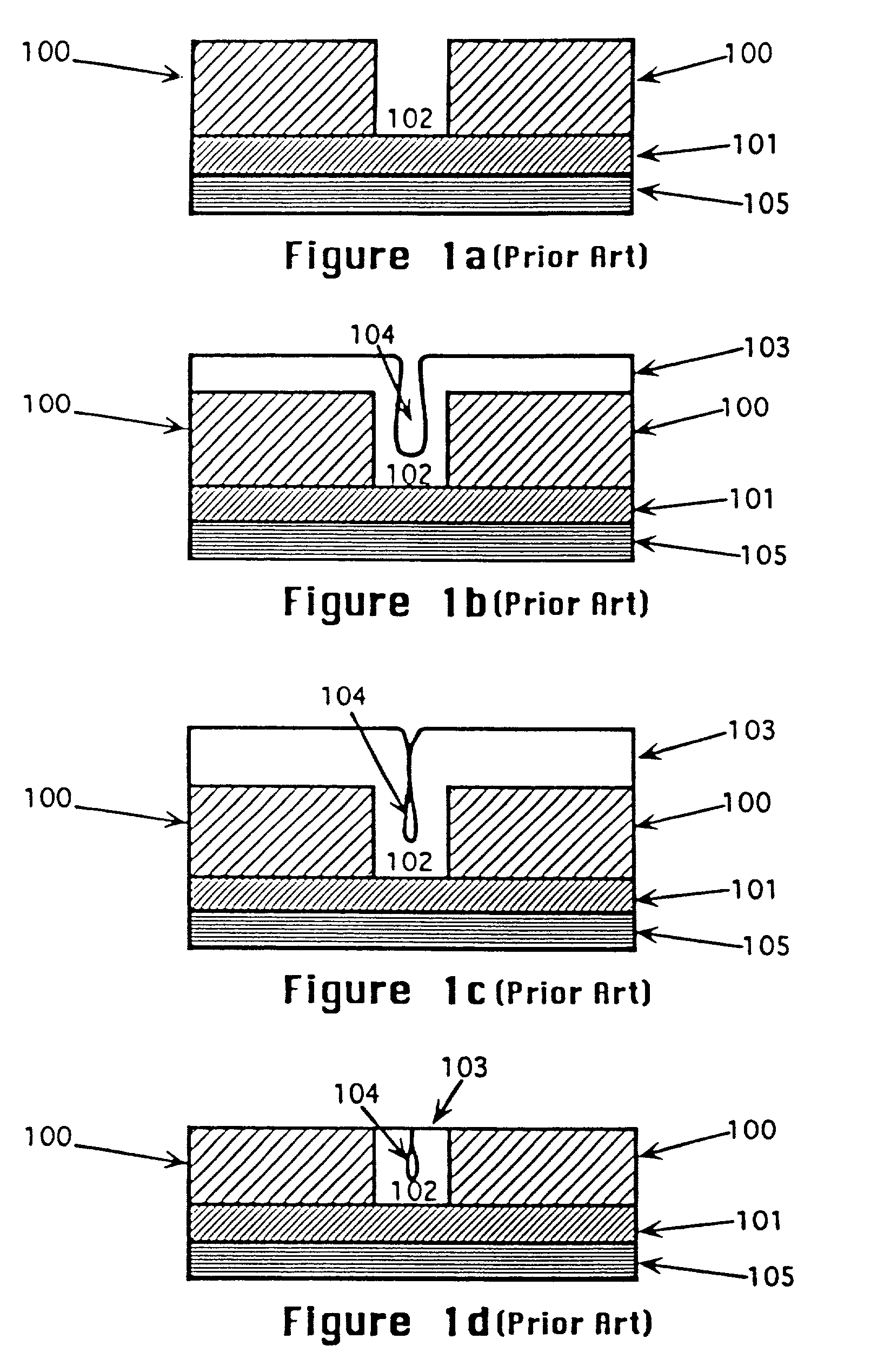
[0031] A manufacturable method for forming a highly reliable, electrical interconnection is described which is particularly well suited for advanced VLSI and ULSI applications. In the following description, numerous specific details such as layer thicknesses, process sequences, times, temperatures, etc. are set forth in order to provide a more thorough understanding of the present invention. It will be obvious, however, to one skilled in the art, that the present invention may be practiced without employing these specific details. In other instances, well-known processes and processing techniques have not been described in detail in order not to unnecessarily obscure the present invention.

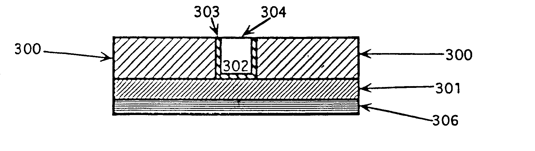
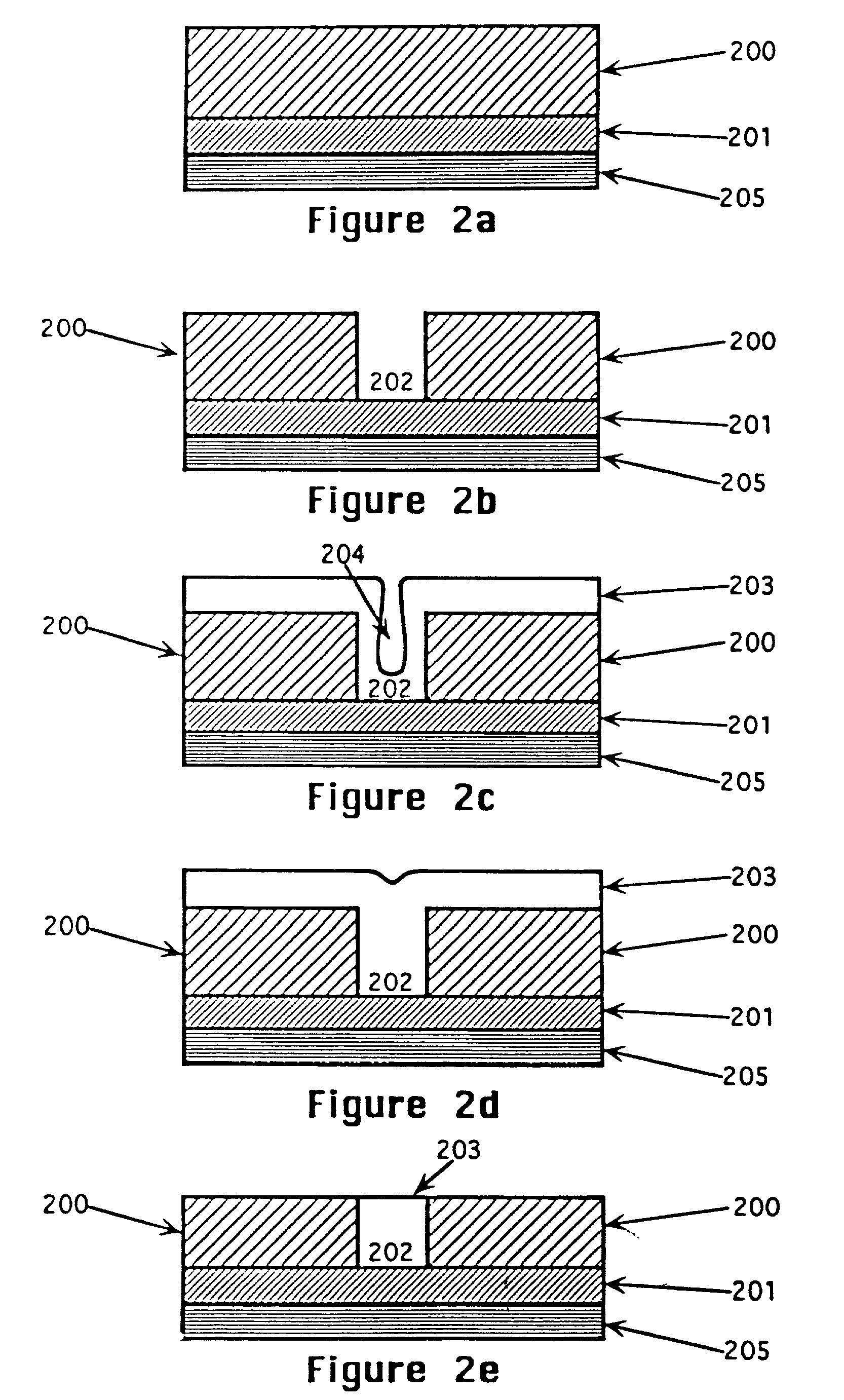
[0032] While diagrams representing a preferred embodiment of the present invention are illustrated in FIGS. 2a-3e, these illustrations are not intended to limit the invention. The specific processes described herein are only meant to help clarify an understanding of the present invention and to ill...


PUM

PropertyMeasurementUnit
temperatureaaaaaaaaaa
widthaaaaaaaaaa

Abstract

A manufacturable method for forming a highly reliable electrical interconnection. An electrical interconnection pattern is first formed in a dielectric layer on a semiconductor substrate as recessed regions in the dielectric layer. A conductive layer primarily comprising copper is thereafter deposited over the surface and in the recessed regions of the dielectric layer. The conductive layer is then reflowed to fill the recessed regions of the dielectric layer with substantially no void formation. This reflow process may also be used to improve the step coverage of any such copper layer deposited over the surface of a substrate to be used in conjunction with alternate techniques for forming electrical interconnections including photoresist patterning and etch.

Description

[0001] The present invention relates to semiconductor processing, and more particularly to a method of forming copper interconnections in a semiconductor device.[0002] As the demand for cheaper, faster, lower power consuming microprocessors increases, so must the device packing density of the integrated circuit. Very large scale integration (VLSI) techniques have continually evolved to meet the increasing demand. All aspects of the integrated circuit must be scaled down to fully minimize the device dimensions of the integrated circuit. In addition to minimizing transistor dimensions, one must minimize the dimensions of the electrical interconnections which integrate the semiconductor devices, such as transistors, together on a microchip in order to form a complete circuit.[0003] Currently, aluminum alloys are the most commonly used conductive materials for electrical interconnections in a VLSI integrated circuit. Aluminum and its alloys have been fully characterized for use as elect...

Claims


Application Information

Patent Timeline
Patent Type & Authority Applications(United States)
IPC IPC(8): H01L21/768
CPCH01L21/76882
Inventor GARDNER, DONALD S.
Owner INTEL CORP
Why Eureka
Try Eureka