
Liquid crystal display panel and liquid crystal display apparatus
a liquid crystal display panel and display panel technology, applied in the field of display panel and display apparatus, can solve the problems of image sticking and reduce production yield, and achieve the effect of reducing light leakage and reducing rubbing mura
- Summary
- Abstract
- Description
- Claims
- Application Information
AI Technical Summary
Benefits of technology
Problems solved by technology
Method used
Image

Examples
first embodiment
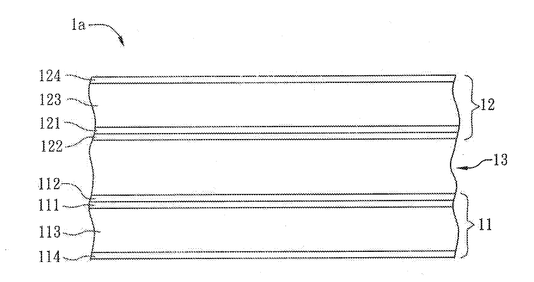
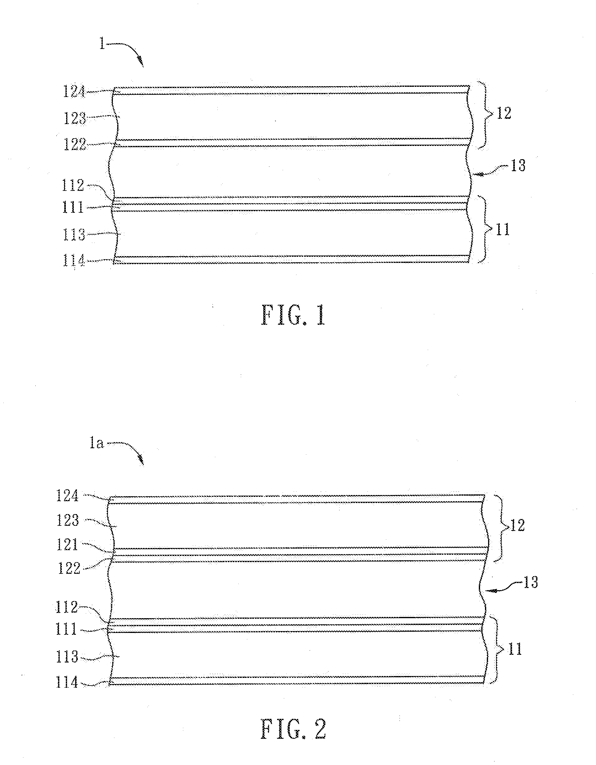
[0036]FIG. 1 is a schematic diagram of a liquid crystal display (LCD) panel 1 according to this disclosure. In the embodiments of this disclosure, the LCD panel 1 is not limited in type, which can be a display panel of a fringe field switching (FFS) type, an in-plane switching (IPS) type, or a vertical alignment (VA) type, for example. The LCD panel 1 includes a first substrate 11, a second substrate 12 and a liquid crystal layer 13. The first and second substrates 11 and 12 are disposed oppositely, and the liquid crystal layer 13 is disposed between the first and second substrates 11 and 12. The first and second substrates 11 and 12 are the combination of a color filter (CF) substrate and a thin film transistor (TFT) substrate. Herein for example, the first substrate 11 is a thin film transistor substrate while the second substrate 12 is a color filter substrate. Besides, the LCD panel 1 can have variations according to other technologies. For example, the color filter layer can be...
second embodiment
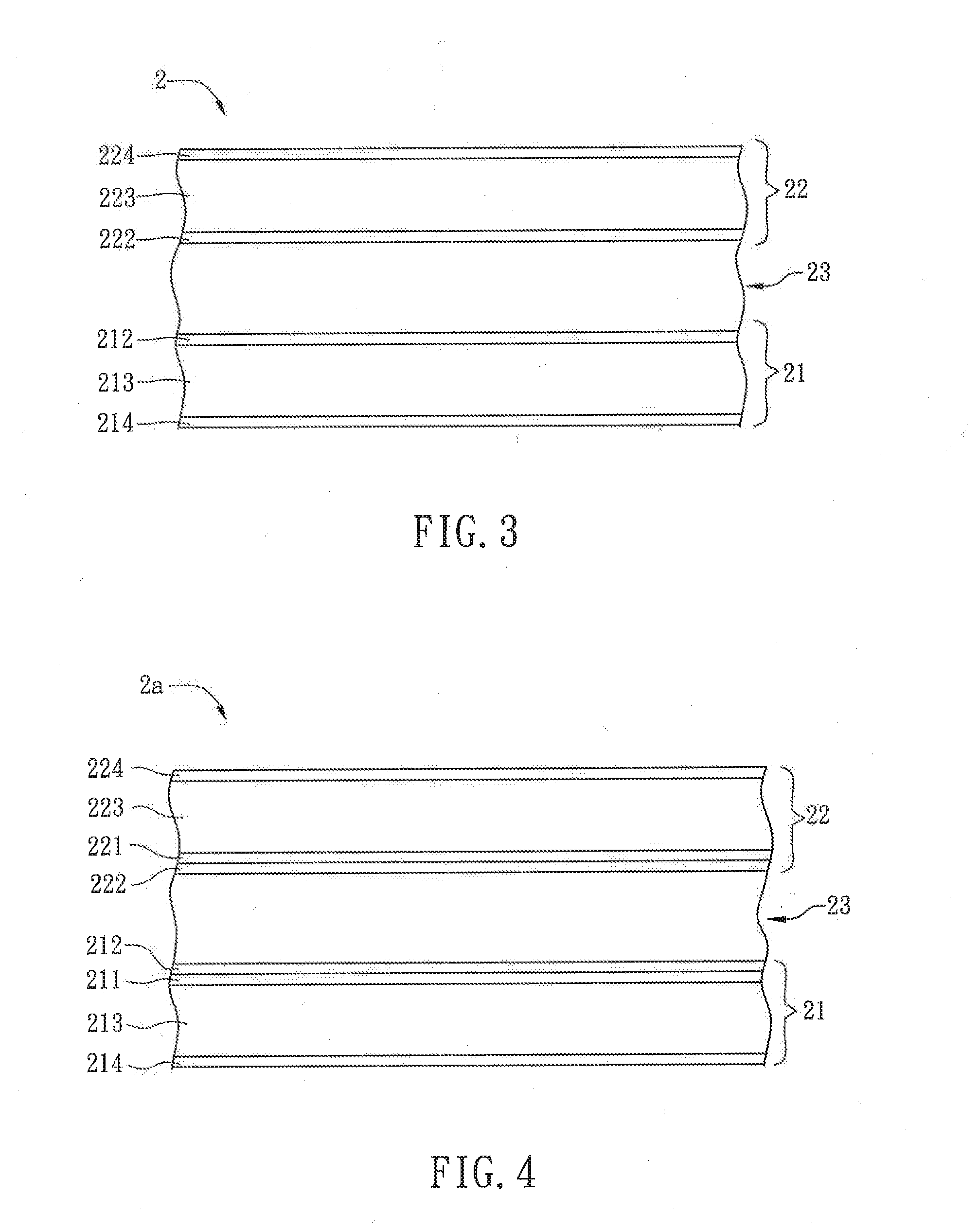
[0053]FIG. 3 is a schematic diagram of a liquid crystal display (LCD) panel 2 according to this disclosure. The LCD panel 2 is not limited in type, which can be a display panel of a fringe field switching (FFS) type, an in-plane switching (IPS) type, or a vertical alignment (VA) type, for example. The LCD panel 2 includes a first substrate 21, a second substrate 22 and a liquid crystal layer 23. The first and second substrates 21 and 22 are disposed oppositely, and the liquid crystal layer 23 is disposed between the first and second substrates 21 and 22. The first and second substrates 21 and 22 are the combination of a color filter (CF) substrate and a thin film transistor (TFT) substrate. Herein for example, the first substrate 21 is a thin film transistor substrate while the second substrate 22 is a color filter substrate. Besides, the LCD panel 2 can have variations according to other technologies. For example, the color filter layer can be disposed to the TFT substrate (i.e. co...
PUM
| Property | Measurement | Unit |
|---|---|---|
| Length | aaaaa | aaaaa |
Abstract
Description
Claims
Application Information