Method and system for smart contact arrays

a technology of contact arrays and smart contacts, applied in the direction of coupling device connections, semiconductor/solid-state device details, instruments, etc., can solve the problems of significant manufacturing cost of cables and connectors, and achieve the effects of improving lifestyle and convenience, light weight and less cos

Active Publication Date: 2014-03-06
I BLADES
View PDF15 Cites 80 Cited by
  • Summary
  • Abstract
  • Description
  • Claims
  • Application Information

AI Technical Summary

Benefits of technology

[0027]A further benefit provided by embodiments of the present invention is that a user may carry or own fewer discrete devices, while improving their lifestyle and convenience. Each of the discrete devices may comprise an odd sized box, each box containing a power supply and a separate controller. The boxes may be bulky. The stacked devices may be smaller and lighter. Thus a user may create a personalized electronic ecosystem that is light weight and convenient.
[0028]The multiple power supplies and controllers may be implemented as a single battery and a single controller provided in a single base module. Each of the required functions may be implemented in a blade module that is then coupled to the base module, or to the stack containing the base module. This efficient allocation of resources may enable the stacked versions to be less expensive than the discrete ones they replace. Furthermore, a library of selectable blade modules may bring to users new flexibility in how they obtain and use devices. They may be rented or leased for example, instead of purchased, and the user may be assured of device compatibility because of the standard coupling interface employed. Using a standardized smart interface element in each device enables the convenience of interoperability between any pair of devices. Additionally, the coupling and uncoupling of devices may be “hot swappable,” providing further convenience to the user by reducing or eliminating shut down procedures in many cases. Furthermore, an ecosystem of electronic devices that are physically connected rather than wirelessly connected, according to many embodiments described herein, may be more secure and less vulnerable to malicious attacks.

Problems solved by technology

Cables and connectors each have a significant manufacturing cost.

Method used


Image

  • Method and system for smart contact arrays
  • Method and system for smart contact arrays
  • Method and system for smart contact arrays

Examples


Embodiment Construction

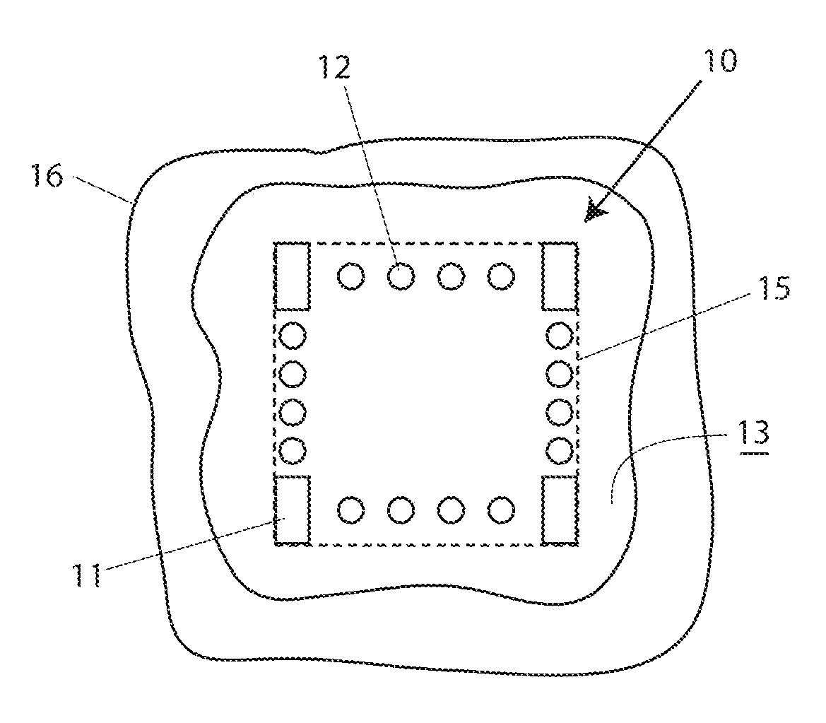
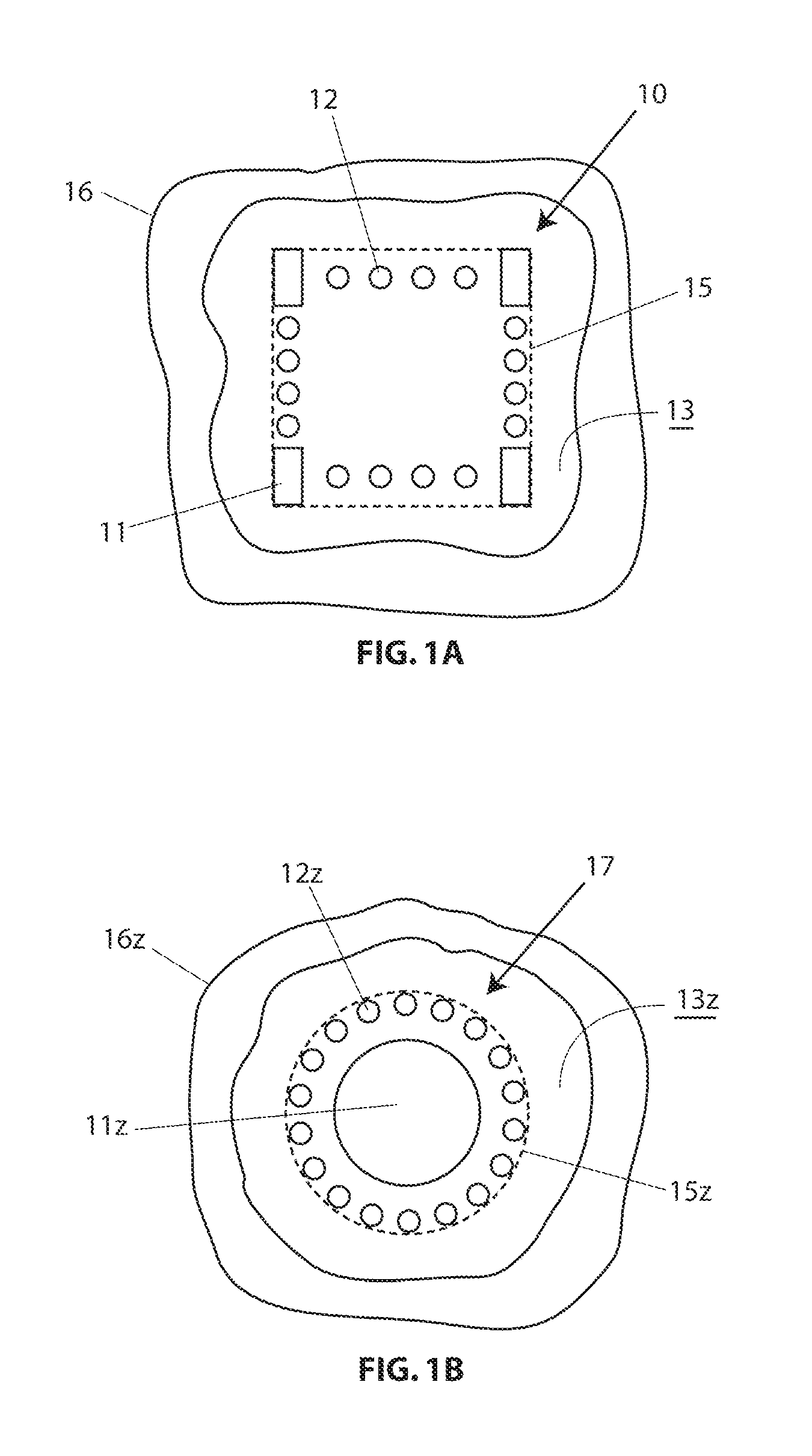
[0072]FIG. 1A shows a plan view of a coupling face 13 of a device, depicting contact array 10 comprising four magnets 11 and sixteen terminals 12. Coupling face 13 has an associated coupling area 15, including a periphery around magnets 11 and terminals 12, and is contained within a body 16 of a device as shown. The magnets 11 are configured so as to provide a coupling force between host devices equipped with like contact arrays. A host device may be defined as any device to which a second device or module may be coupled. A type of rare earth magnet called a “neodymium magnet” comprises Neodymium (Nd), Iron (Fe) and Boron (B), and a suitable magnet size for the contact array may be around 4 mm×2 mm×1 mm. Any type of magnet may be used, including an electromagnet, typically comprised of an iron core and a winding, wherein the electromagnet is activated by passing a current through the winding. Opposing contact arrays comprising four such magnets in each host device may have a breakaw...


PUM

PropertyMeasurementUnit
currentaaaaaaaaaa
sizeaaaaaaaaaa
thickaaaaaaaaaa

Abstract

A device includes a device body having an attachment face defined by an attachment area and a contact array disposed in the device body and exposed at a coupling face. The contact array comprises one or more magnets disposed on the coupling face and a plurality of terminals disposed on the coupling face. A periphery of the one or more magnets and the plurality of terminals defines a coupling area. The attachment area is greater than and independent of the coupling area.

Description

CROSS-REFERENCES TO RELATED APPLICATIONS[0001]This application claims priority to U.S. Provisional Patent Application Nos. 61 / 696,245, filed on Sep. 3, 2012, entitled “Magnetically and Electrically Coupled Devices, 61 / 708,730, filed on Oct. 2, 2012, entitled “Magnetically and Electrically Coupled Devices,”, 61 / 751,936, filed on Jan. 13, 2013, entitled “Magnetically and Electrically Coupled Devices, 61 / 803,494, filed on Mar. 20, 2013, entitled, “Method and Apparatus for Trusted Pairs and Private Networks, 61 / 807,609, filed on Apr. 2, 2013, entitled “Protocol Converter Module, 61 / 823,071, filed on May 14, 2013, entitled “Snap On Module Interface, 61 / 840,529, filed on Jun. 28, 2013, entitled “Magnetically Attached Chip Package, and 61 / 844,006, filed on Jul. 9, 2013, entitled “Snap On Wearable Module, the disclosures of which are hereby incorporated by reference in their entirety for all purposes.[0002]The following regular U.S. patent applications (including this one) are being filed c...

Claims


Application Information

Patent Timeline
Patent Type & Authority Applications(United States)
IPC IPC(8): H01R13/62H05K13/00H04M1/724H04M1/72412
CPCH05K13/00H01R13/6205H04M1/0256H01L2224/16225H01L2224/48465H01L2224/73265Y10T29/49002Y10T29/49117H04M1/72412H01L2224/32245H01L2224/48247H01L2924/00G07C9/25G07C9/20H04M1/724G07C9/00182G07C2009/00206H01L23/49513H01L23/49541H01L24/32H01L2224/16245H01L2224/48091H01L2224/48106H01R24/86H01R43/26H01R2107/00
Inventor SALMON, PETER C.FERNANDES, JORGEMEISSNER, PAULPANAGROSSI, JERRY
Owner I BLADES
Why Eureka
Try Eureka