Volatile/non-volatile memory cell

a memory cell, non-volatile technology, applied in the direction of logic circuit coupling/interface arrangement, pulse technique, instruments, etc., can solve the problems of requiring a relatively high supply voltage, and affecting the operation of the devi

Active Publication Date: 2014-03-13
CENT NAT DE LA RECHERCHE SCI +1
View PDF5 Cites 5 Cited by
  • Summary
  • Abstract
  • Description
  • Claims
  • Application Information

AI Technical Summary

Benefits of technology

[0007]It is an aim of embodiments of the present invention to at least partially address one or more needs in the prior art.

Problems solved by technology

However, a disadvantage is that, as with all volatile memory cells, the stored data is lost if the supply voltage VDD is removed.
A disadvantage with flash memory is that it is relatively slow to access when compared to the SRAM cell of FIG. 1, and requires a relatively high supply voltage.
Furthermore, the Flash technology is difficult to integrate with CMOS, and has relatively low endurance.

Method used


Image

  • Volatile/non-volatile memory cell
  • Volatile/non-volatile memory cell
  • Volatile/non-volatile memory cell

Examples


Embodiment Construction

[0039]Only those features useful for an understanding of the invention have been illustrated in the figures and will be described in detail in the following. Other aspects, such as the particular applications of the memory cell, have not been described, the memory cell being suitable for use in a wide range of applications.

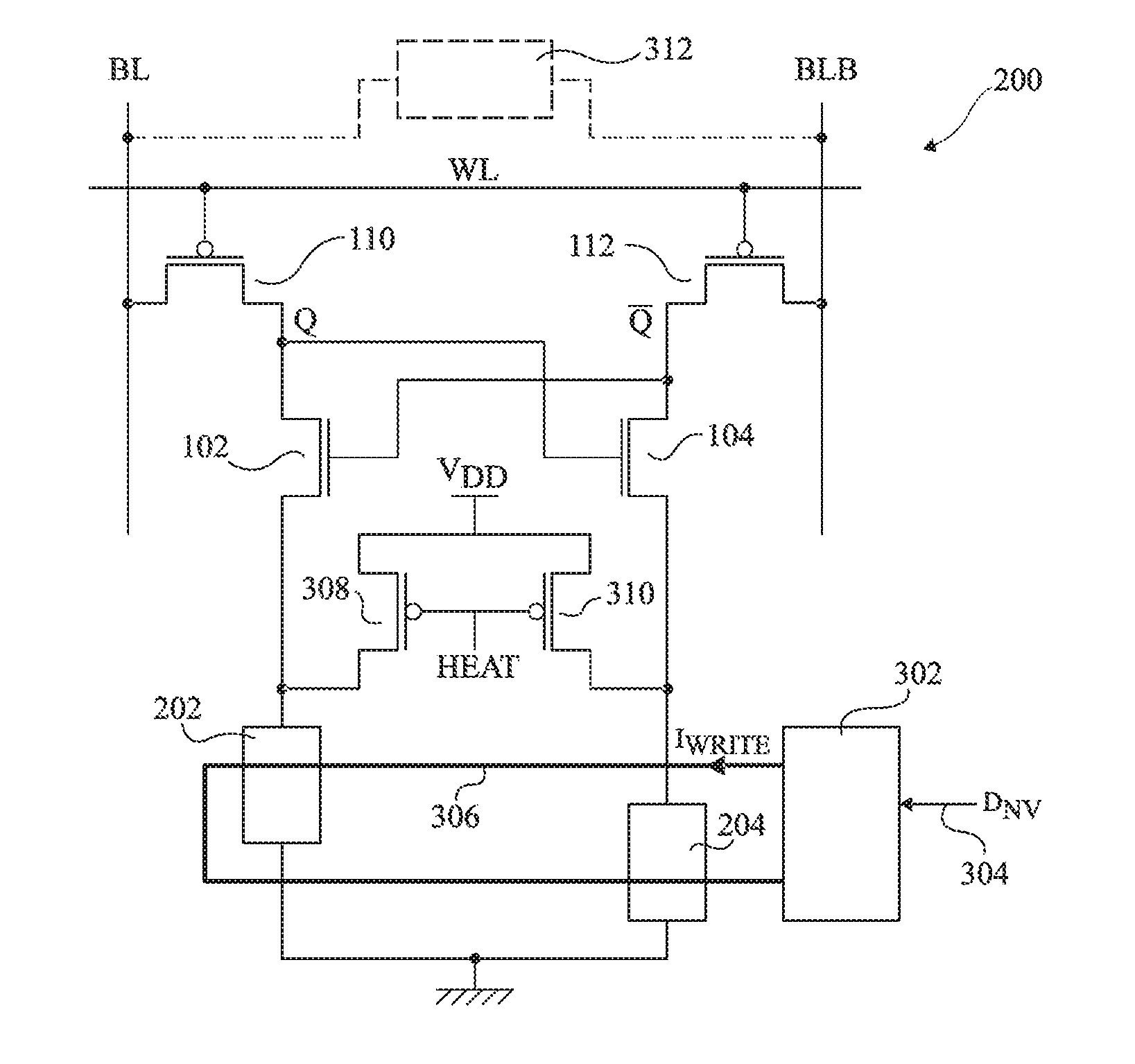
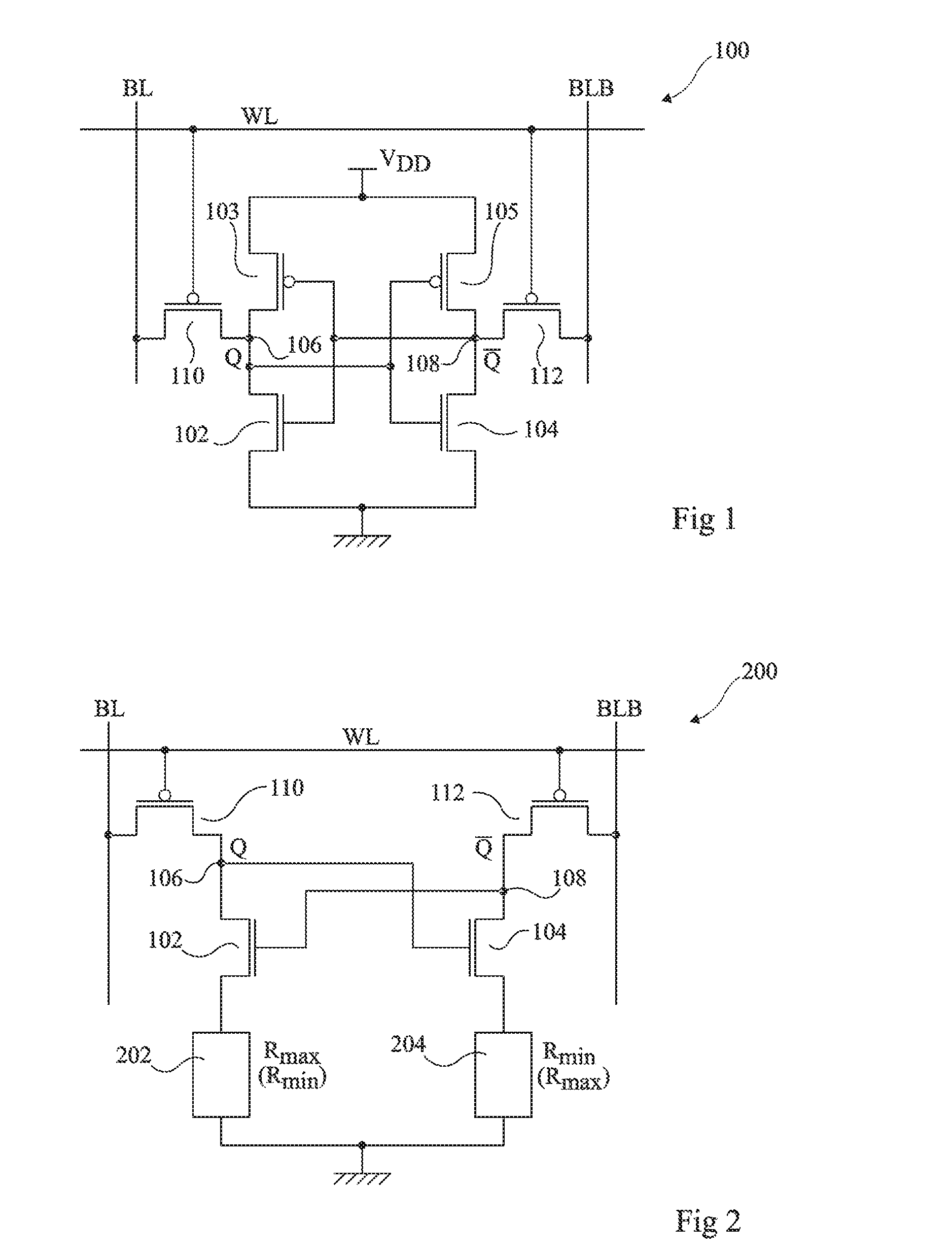
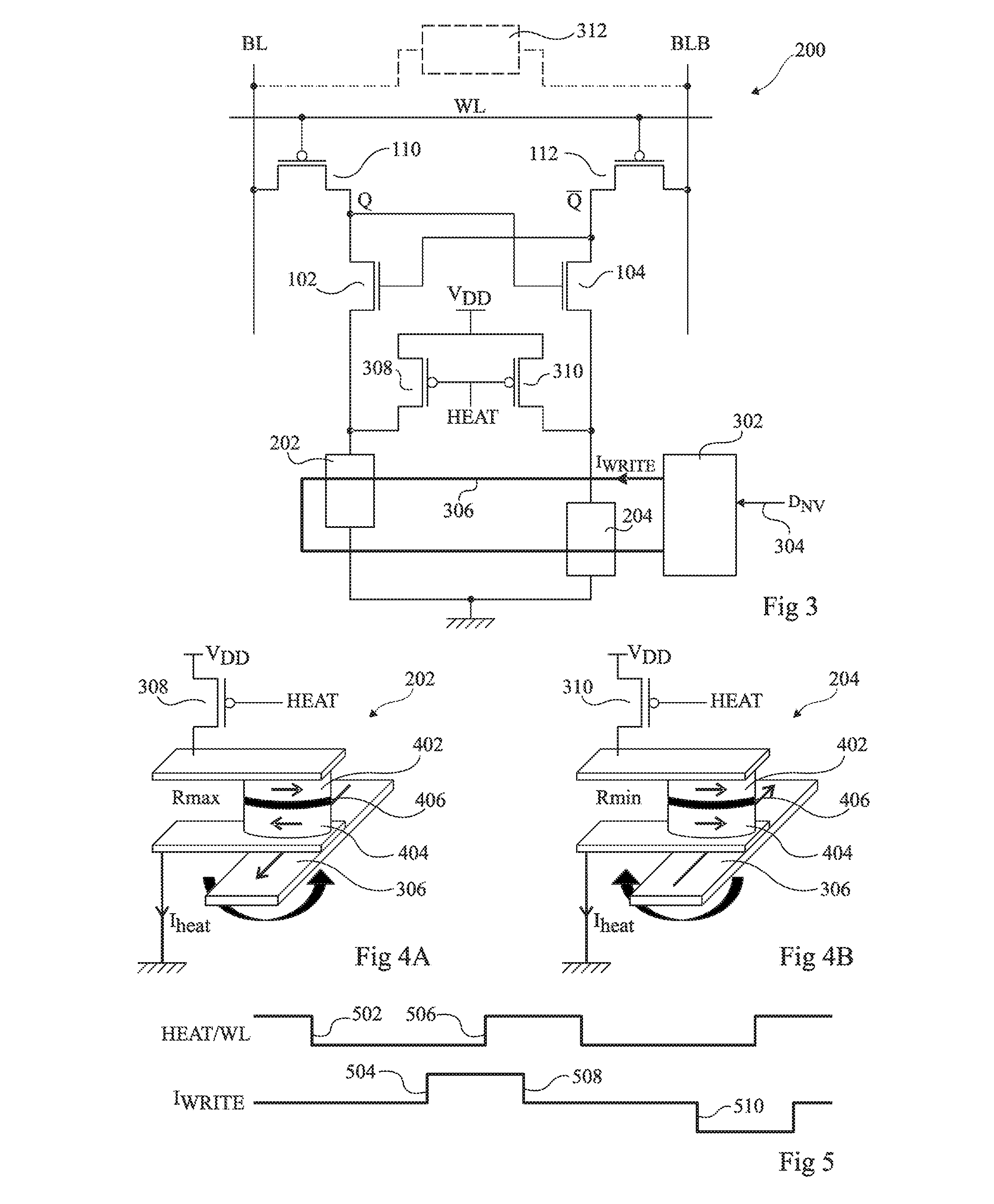
[0040]FIG. 2 illustrates a memory cell 200 that stores, in addition to one bit of volatile data, one bit of non-volatile data. The volatile data is stored in electronic form by a latch. The non-volatile data however is stored by the physical state of a pair of resistance switching elements, as will now be described.

[0041]The memory cell 200 is similar to the SRAM cell 100 of FIG. 1 described above, and the common portions will not be described again in detail. However, rather than comprising six transistors, the memory cell 200 comprises just four transistors. Indeed, the PMOS transistors 103 and 105 forming half of each inverter are removed, and thus there is no ...


PUM


Abstract

The invention concerns a memory device comprising at least one memory cell comprising: a first transistor (102) coupled between a first storage node (106) and a first resistance switching element (202) programmed to have a first resistance; and a second transistor (104) coupled between a second storage node (108) and a second resistance switching element (204) programmed to have a second resistance, a control terminal of said first transistor being coupled to said second storage node, and a control terminal of said second transistor being coupled to said first storage node; and control circuitry (602) adapted to store a data value (DNV) at said first and second storage nodes by coupling said first and second storage nodes to a first supply voltage (VDD, GND), the data value being determined by the relative resistances of the first and second resistance switching elements.

Description

FIELD OF THE INVENTION[0001]The present invention relates to a programmable volatile / non-volatile memory cell, and to a method of reading a programmable non-volatile memory cell.BACKGROUND OF THE INVENTION[0002]FIG. 1 illustrates a typical static random access memory (SRAM) cell 100. A first inverter is formed of an N-channel MOS (NMOS) transistor 102 and P-channel MOS (PMOS) transistor 103 coupled in series between a supply voltage VDD and a ground voltage. A second inverter is formed of an NMOS transistor 104 and a PMOS transistor 105 also coupled in series between the supply voltage VDD and the ground voltage. The gates of transistors 104 and 105 are coupled to a node 106 coupled to the drains of transistors 102 and 103, while the gates of transistors 102 and 103 are coupled to a node 108 coupled to the drains of transistors 104 and 105, such that the inverters form a latch.[0003]The nodes 106 and 108 store complementary voltage states Q and Q, permitting one bit of data to be me...

Claims


Application Information

Patent Timeline
Patent Type & Authority Applications(United States)
IPC IPC(8): G11C13/00H03K19/0175
CPCH03K19/017581G11C13/0069G11C11/15G11C11/412G11C13/0002G11C11/1659G11C14/0081G11C11/1675G11C11/1693G11C14/009G11C11/16
Inventor GUILLEMENET, YOANNTORRES, LIONELPRENAT, GUILLAUMETORKI, KHOLDOUNDI PENDINA, GREGORY
Owner CENT NAT DE LA RECHERCHE SCI
Why Eureka
Try Eureka