
Method and Apparatus for Improving Particle Performance

Inactive Publication Date: 2014-03-27
INTERMOLECULAR
View PDF0 Cites 158 Cited by
  • Summary
  • Abstract
  • Description
  • Claims
  • Application Information

AI Technical Summary

Benefits of technology

The patent is about a device that reduces the generation of particles when processing a semiconductor substrate. The device has several embodiments. The technical effect is to minimize the production of particles that can contaminate the semiconductor device being made.

Problems solved by technology

This approach has resulted in ever escalating R&D costs and the inability to conduct extensive experimentation in a timely and cost effective manner.

Method used


Image

  • Method and Apparatus for Improving Particle Performance
  • Method and Apparatus for Improving Particle Performance
  • Method and Apparatus for Improving Particle Performance

Examples


Embodiment Construction

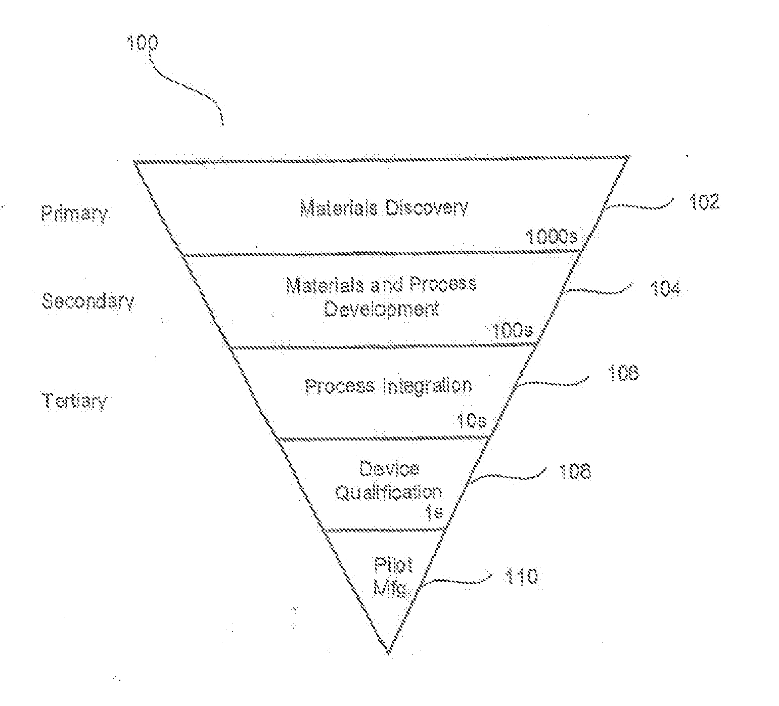
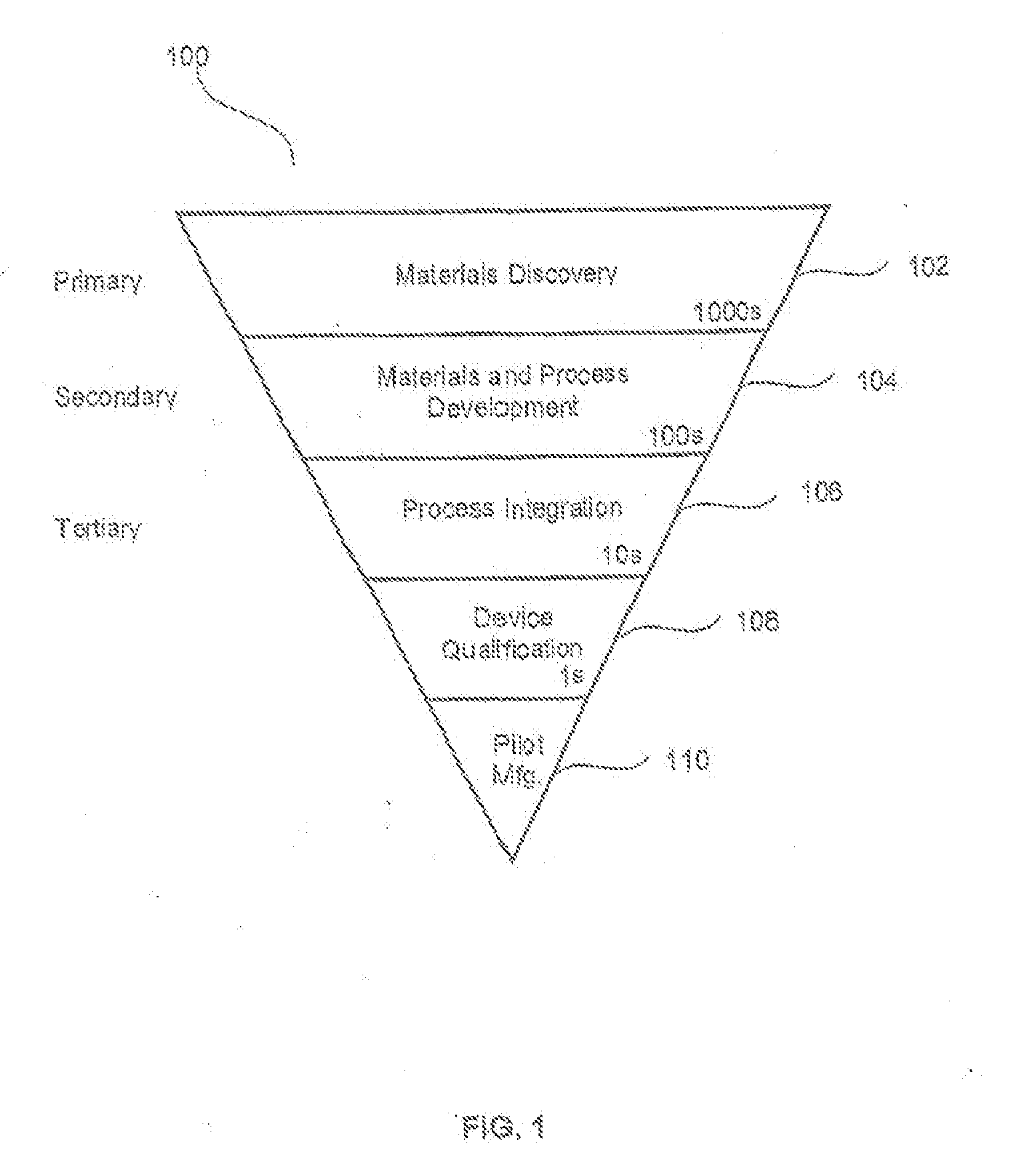
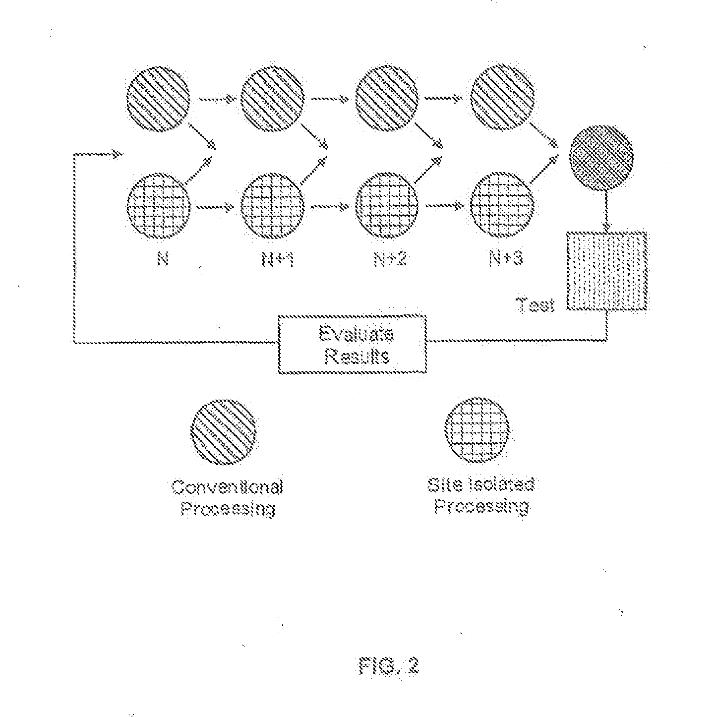
[0017]The embodiments described herein provide a method and apparatus for a combinatorial processing system providing for control of a sealing pressure between a reactor and a substrate. It will be obvious, however, to one skilled in the art, that the present invention may be practiced without some or all of these specific details. In other instances, well known process operations have not been described in detail in order not to unnecessarily obscure the embodiments.

[0018]The embodiments describe a method for controlling the abrasion of sleeve sealing surfaces with substrate surfaces in the F-30 module of the assignee or other suitable processing equipment during clamping and unclamping operations in order to minimize leaks and particle generation. In the embodiments described below, the sleeves have a top portion that locks into place rigidly with the reactor block rather than seal against an o-ring, which is compressible and limits the control of abrasion of the sealing surface o...


PUM


Abstract

A method for combinatorially processing a substrate is provided. The method includes providing a substrate disposed on a substrate support. The method further includes rigidly locking a top portion of a sleeve to a bottom portion of a process head of a combinatorial processing device, where the combinatorial processing device is operable to concurrently process different regions of the substrate differently. The method includes raising the substrate and the substrate support to contact a sealing surface of the sleeve with a surface of the substrate and combinatorially processing the different regions of the substrate.

Description

BACKGROUND[0001]Combinatorial processing provides high throughput evaluation of semiconductor processes and materials. The systems supporting the combinatorial processing are flexible to accommodate the demands for running the different processes either in parallel, serial or some combination of the two.[0002]Some semiconductor wet processing operations include operations for adding (electro-depositions) and removing layers (etch), defining features, preparing layers (e.g., cleans), etc. Similar processing techniques apply to the manufacture of integrated circuits (IC) semiconductor devices, flat panel displays, optoelectronics devices, data storage devices, magneto electronic devices, magneto optic devices, packaged devices, and the like. As feature sizes continue to shrink, improvements, whether in materials, unit processes, or process sequences, are continually being sought for the deposition processes. However, semiconductor companies conduct R&D on full wafer processing through...

Claims


Application Information

Patent Timeline
IPC IPC(8): H01L21/66
CPCH01L22/10H01L21/6719
Inventor KAHLON, SATBIR
Owner INTERMOLECULAR
Features
  • Generate Ideas
  • Intellectual Property
  • Life Sciences
  • Materials
  • Tech Scout
  • Unparalleled Data Quality
  • Higher Quality Content
  • 60% Fewer Hallucinations
Learn More