Optical filter, solid-state imaging element, imaging device lens and imaging device

Active Publication Date: 2014-04-03
ASAHI GLASS CO LTD
View PDF4 Cites 86 Cited by
  • Summary
  • Abstract
  • Description
  • Claims
  • Application Information

AI Technical Summary

Benefits of technology

[0057]According to the present invention, it may be possible to obtain an optical filter, a solid-state imaging element, and a lens, each of which when used solely or in combination with other selective

Problems solved by technology

However, light absorption type glass filters involved such a problem that not only they are expensive, but also they are difficult to achieve slimming, so that they may be impossible to sufficiently respond to downsizing and slimming requirements for imaging devices of recent years.
However, in these conventional optical filters for imaging device, the performance for shielding light of a wavelength in a near infrared region and the transmission properties in a wavelength band (630 to 7

Method used


Image

  • Optical filter, solid-state imaging element, imaging device lens and imaging device
  • Optical filter, solid-state imaging element, imaging device lens and imaging device
  • Optical filter, solid-state imaging element, imaging device lens and imaging device

Examples


first embodiment

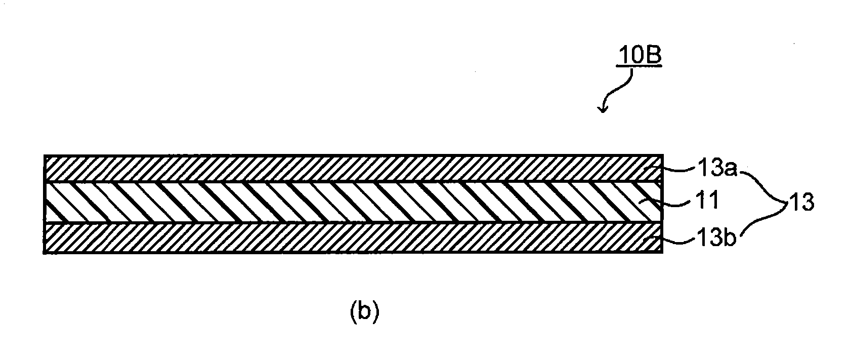
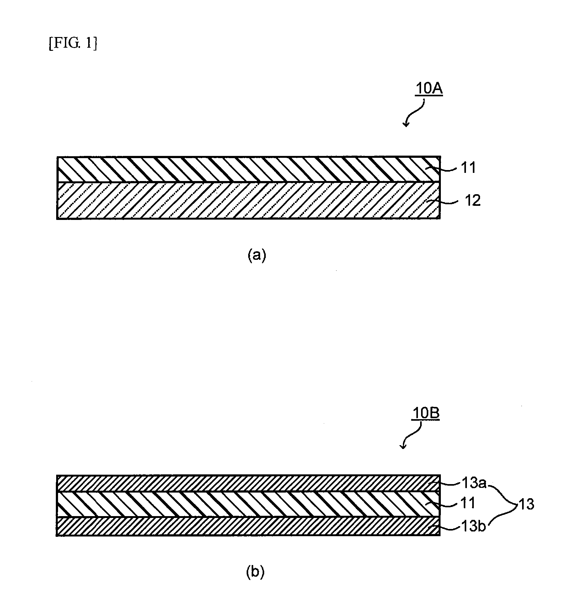
[0070]The present embodiment is concerned with an optical filter containing a near infrared ray absorbing layer having the following near infrared ray absorbing dye (A) dispersed in a transparent resin (B) having a refractive index (n20d) of 1.54 or more, in which the near infrared ray absorbing layer has a transmittance of visible light of from 450 to 600 nm of 70% or more, a transmittance of light in a wavelength region of from 695 to 720 nm of not more than 10%, and an amount of change D of transmittance expressed by the foregoing equation (1) of not more than −0.8. Incidentally, in the present description, the refractive index refers to a refractive index (n20d), unless otherwise indicated.

[0071]The near infrared ray absorbing dye (A) used in the present embodiment contains a near infrared ray absorbing dye (A1) having a maximum absorption peak such that in an absorption spectrum of light in a wavelength region of from 400 to 1,000 nm as measured upon being dissolved in a solven...

second embodiment

[0250]FIG. 3 is a cross-sectional view showing diagrammatically a part of a solid-state imaging element according to the present embodiment. The solid-state imaging element of the present embodiment is a solid-state imaging element used for an imaging device such as a small-sized camera, etc., which is installed in an information appliance such as a digital still camera, a digital video camera, a mobile phone, a laptop computer, PDA (personal digital assistance), etc. In the following embodiments, in order to avoid overlapping explanations, the points common to those in the first embodiment are omitted under certain circumstances, and the explanation is made centering on different points.

[0251]As shown in FIG. 3, in this solid-state imaging element 20A, a flattened layer 104, a color filter layer 105, and a microlens 106 are provided in this order on a semiconductor substrate 103 such as a silicon substrate, etc, having a photoelectric conversion element 101 and a light shielding la...

third embodiment

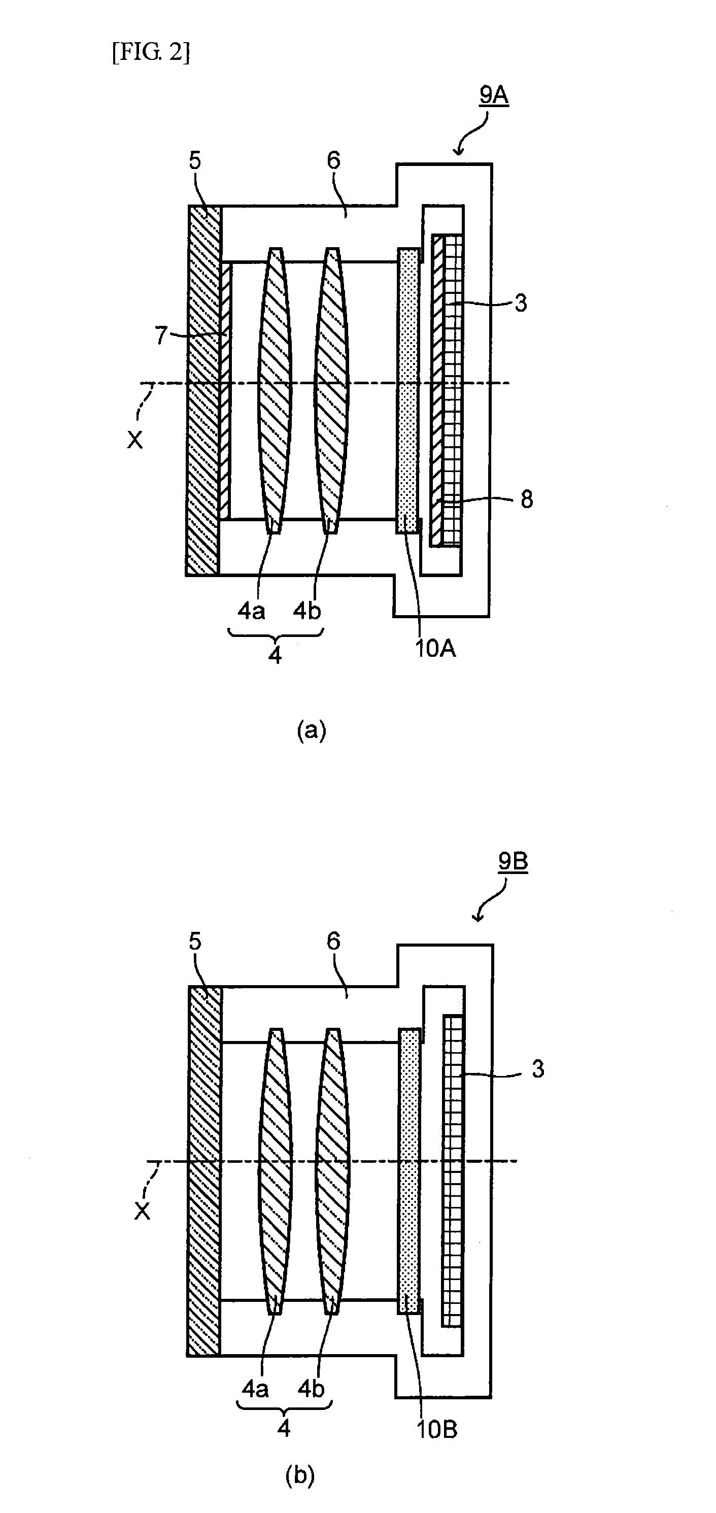
[0275]FIG. 5 is a cross-sectional view showing an imaging device lens according to the present embodiment. This imaging device lens is a lens configuring the whole or a part of a lens system to be subjected to image formation into the solid-state imaging element in an imaging device such as a small-sized camera, etc., which is installed in an information appliance such as a digital still camera, a digital video camera, a mobile phone, a laptop computer, PDA, etc.

[0276]In an imaging device lens 70A shown in FIG. 5, a glass concavo-convex lens in which a one-sided surface 71a has a concave surface, and the other surface 71b has a convex surface and which has a flat plate part 74 in the periphery thereof is used as a lens main body 71. A near infrared ray absorbing layer 72 in which similar to the above-described optical filter, the NIR absorbing dye (A) is dispersed in the transparent resin (B) is provided on the surface 71a on the concave surface side of this glass concavo-convex len...


PUM

PropertyMeasurementUnit
Fractionaaaaaaaaaa
Fractionaaaaaaaaaa
Fractionaaaaaaaaaa

Abstract

The present invention relates to an optical filter, a solid-state imaging element and an imaging device lens which contain a near infrared ray absorbing layer having a specific near infrared ray absorbing dye dispersed in a transparent resin having a refractive index of 1.54 or more, and also relates to an imaging device containing the solid-state imaging element or the imaging device lens. The near infrared ray absorbing layer has a transmittance of visible light of from 450 to 600 nm of 70% or more, a transmittance of light in a wavelength region of from 695 to 720 nm of not more than 10%, and an amount of change of transmittance of not more than −0.8

Description

TECHNICAL FIELD[0001]The present invention relates to an optical filter, a solid-state imaging element and an imaging device lens, which have a near infrared ray shielding effect, and it also relates to an imaging device using the same.BACKGROUND ART[0002]In recent years, optical filters that sufficiently transmit light in a visible wavelength region therethrough but shield light in a near infrared wavelength region are used for various applications.[0003]For example, in imaging devices using a solid-state imaging element (e.g., CCD, CMOS, etc.), such as a digital still camera, a digital video camera, etc., or in display devices using a light receiving element, such as an automatic exposure meter, etc., in order to approximate the sensitivity of the solid-state imaging element or light receiving element to the luminosity factor of a human being, such an optical filter is disposed between an imaging lens and the solid-state imaging element or light receiving element. In addition, in ...

Claims


Application Information

Patent Timeline
IPC IPC(8): G02B5/20G02B5/28H01L27/146G02B1/04
CPCG02B5/208H01L27/14621G02B5/282G02B1/04C09B23/086G02B13/004C09B57/007C09B23/107G02B5/223G02B13/005
Inventor HASEGAWA, MAKOTOKASHIWABARA, SATOSHISHIMODA, HIROSHISEKIKAWA, KENTASHIBUYA, TAKASHIOSAWA, MITSUOKAMIJYO, KATSUSHIARISHIMA, HIROYUKIKUMAI, HIROSHI
Owner ASAHI GLASS CO LTD
Why Eureka
Try Eureka