Liquid crystal display and manufacturing method thereof

a technology of liquid crystal display and manufacturing method, which is applied in the direction of optics, instruments, electrical equipment, etc., can solve the problems of reduced aperture ratio and distortion of electric field, and achieve the effect of increasing aperture ratio

Inactive Publication Date: 2014-04-17
SAMSUNG DISPLAY CO LTD
View PDF3 Cites 11 Cited by
  • Summary
  • Abstract
  • Description
  • Claims
  • Application Information

AI Technical Summary

Benefits of technology

[0030]According to exemplary embodiments of the present disclosure, when the sacrificial layer is etched, the common electrode or the etch stop layer formed at the upper portion of the sacrificial layer and etched to narrow the horizontal area occupied by the side wall of the sacrificial layer, and

Problems solved by technology

However, there may be a difficulty in that an aperture ratio is reduced due to a side wall of the EM structure.
Further, a common elect

Method used


Image

  • Liquid crystal display and manufacturing method thereof
  • Liquid crystal display and manufacturing method thereof
  • Liquid crystal display and manufacturing method thereof

Examples


Embodiment Construction

[0041]Exemplary embodiments of the present invention will be described more fully hereinafter with reference to the accompanying drawings, in which exemplary embodiments of the invention are shown.

[0042]In the drawings, the thickness of layers, films, panels, regions, etc., may be exaggerated for clarity. Like reference numerals designate like elements throughout the specification. It will be understood that when an element such as a layer, film, region, or substrate is referred to as being “on” another element, it can be directly on the other element or intervening elements may also be present.

[0043]As used herein, the singular forms, “a”, “an”, and “the” are intended to include plural forms as well, unless the context clearly indicates otherwise.

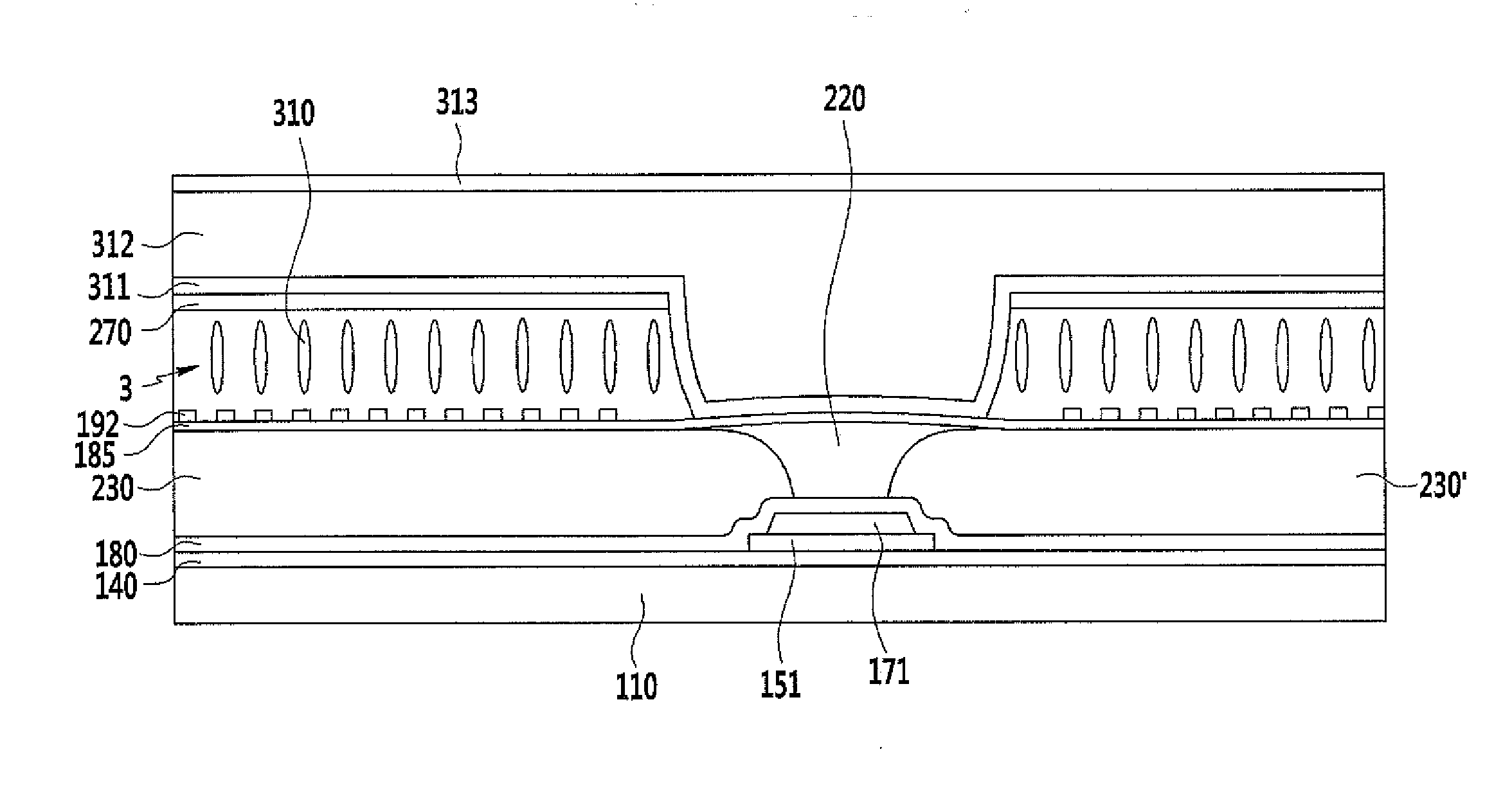
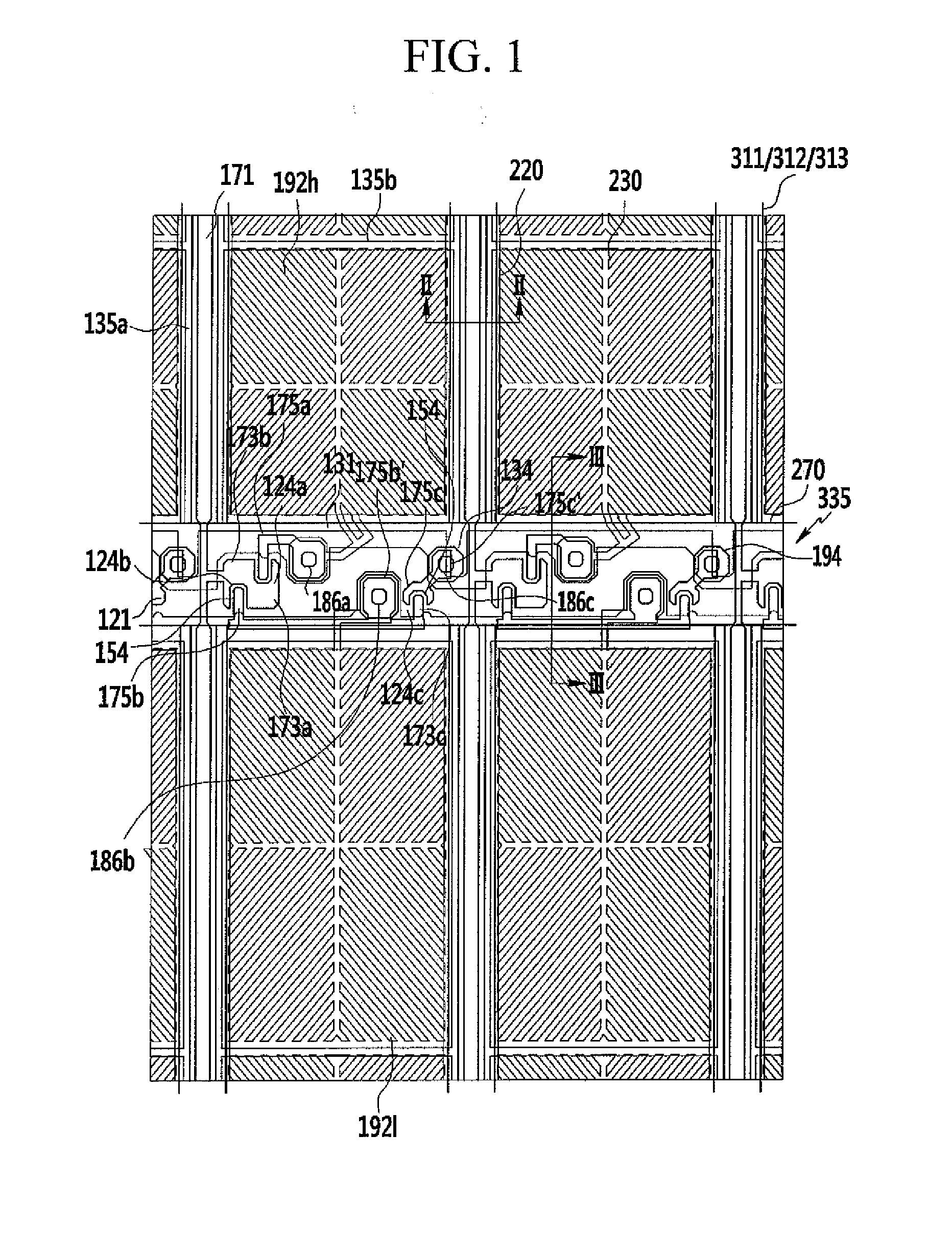
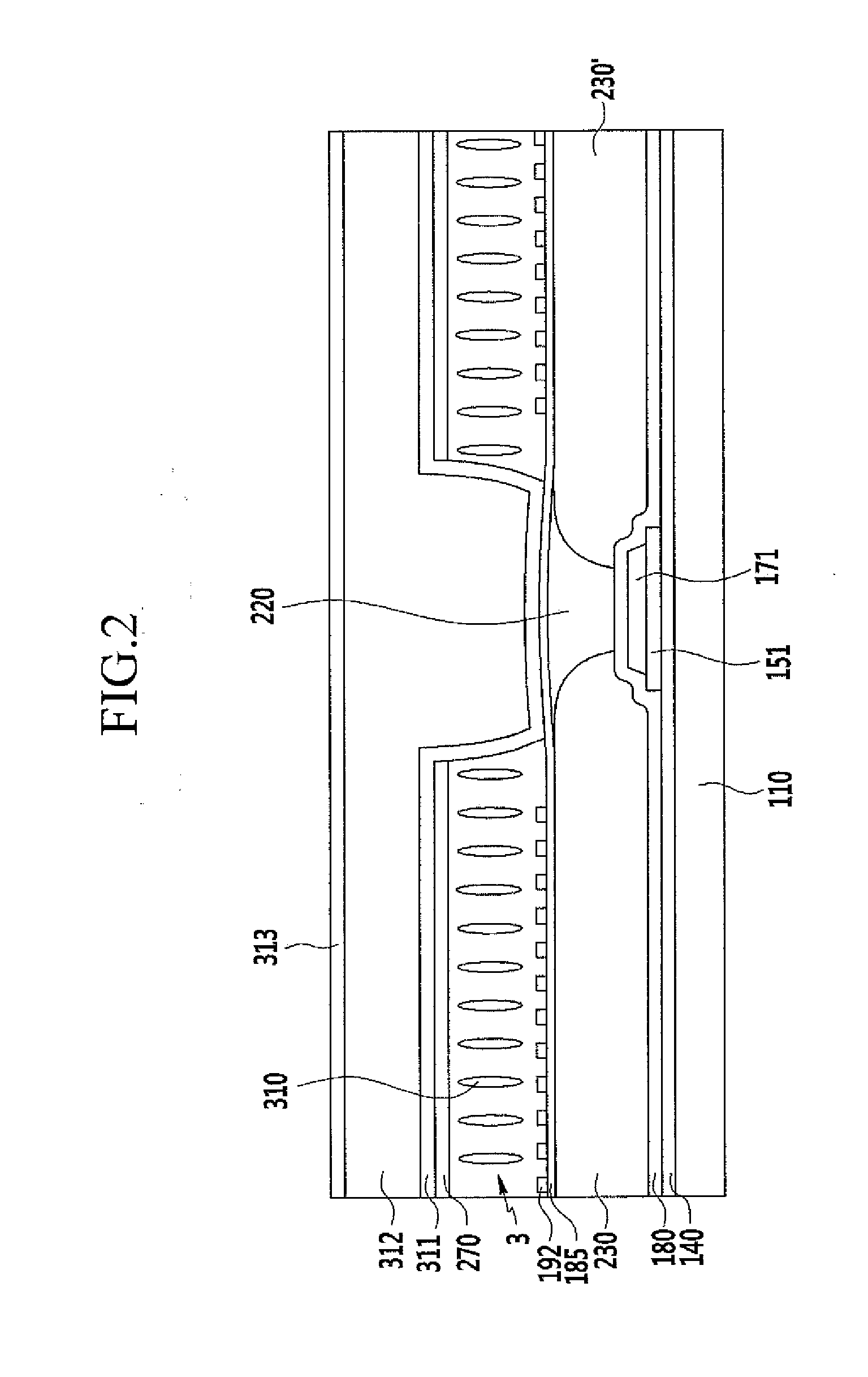
[0044]Hereinafter, a liquid crystal display according to an exemplary embodiment of the present invention will be described with reference to FIGS. 1 to 3.

[0045]FIG. 1 is a layout view of a liquid crystal display according to an exemplary ...


PUM


Abstract

A manufacturing method of a liquid crystal display includes forming a sacrificial layer on a liquid crystal panel, forming an etch stop layer on the sacrificial layer, forming a photo resist pattern on the etch stop layer, completing the etch stop layer using the photo resist pattern as a mask, ashing the photo resist pattern and the sacrificial layer by using the completed etch stop layer as a mask, forming a microcavity by removing a portion of the sacrificial layer and forming a liquid crystal layer in the microcavity.

Description

CROSS-REFERENCE TO RELATED APPLICATION[0001]This application claims priority to Korean Patent Application No. 10-2012-0114226 filed on Oct. 15, 2012, the entire disclosure of which is hereby incorporated by reference herein in its entirety.TECHNICAL FIELD[0002]The present disclosure relates to a liquid crystal display and a manufacturing method thereof, and more particularly, to a liquid crystal display having a liquid crystal layer (nano crystal) included in a microcavity and a manufacturing method thereof.DISCUSSION OF THE RELATED ART[0003]A liquid crystal display which is one of the most common types of flat panel displays currently in use, includes two sheets of panels with field generating electrodes such as a pixel electrode, a common electrode, and the like and a liquid crystal layer interposed therebetween.[0004]The liquid crystal display generates an electric field in the liquid crystal layer by applying voltage to the field generating electrodes, and determines the directi...

Claims


Application Information

Patent Timeline
IPC IPC(8): G02F1/1343
CPCG02F1/134363G02F1/133377G02F1/133707G02F1/136209G02F1/1393G02F1/134345G02F1/1333G02F1/1343
Inventor LEE, SEON UKKIM, WON TAEKIM, YU JINLEE, WOO JAECHAE, KYUNG-TAE
Owner SAMSUNG DISPLAY CO LTD
Why Eureka
Try Eureka