FIR Filter Using Unclocked Delay Elements

Active Publication Date: 2014-04-17
ESS TECHNOLOGY
View PDF4 Cites 2 Cited by
  • Summary
  • Abstract
  • Description
  • Claims
  • Application Information

AI Technical Summary

Benefits of technology

The patent describes a method and system for designing filters that use unclocked digital delay elements to process analog signals. These filters can operate as analog-in / analog-out filters with quantization in the delay line of amplitude but not time. The use of unclocked digital delay simplifies the process of implementing filters and allows for a more efficient and accurate response to the input signal. The system includes a pulse width encoder, delay line, buffers, and elements with impedance values that produce the desired frequency response to the pulse-width encoded signal. The technical effect of this patent is to provide a more efficient and accurate method for filtering analog signals.

Problems solved by technology

Analog filters having well-defined and steep transition bands (the range of frequencies where the filter goes from passing the signal to blocking the signal) can be complex and costly.
The components of such filters may be hard to match, particularly on a single silicon chip because the transfer function, as represented in a pole-zero analysis, requires many poles and / or zeros which must all match.
Some such analog applications, for example a band limiting filter such as a television channel select filter (CSF), may be commonly done with an expensive surface acoustic wave (SAW) device.
However, such devices may have reliability issues due to the need to interconnect from the SAW device to a silicon chip, as well as insertion losses, which typically require a high performance amplifier to compensate.
However, one limitation on an “all analog” FIR filter is the delay elements: although a transmission line is an easy way to implement such delay elements, such a line is impractical to implement on a silicon chip.
But ΣΔ modulators have their own issues.
While this is not too fast for a clock, it is too fast for the filter, which must be analog and must operate with accuracy of about one part in 1000.
However, such a band-pass ΣΔ modulator demands a precision filter in its noise shaping loop.
Thus, a CSF based on a band-pass ΣΔ modulator and a semi-analog FIR filter may become just as complex and costly as a more conventional CSF built with high order analog filter components or with SAW devices, and thus may not be commercially viable.

Method used


Image

  • FIR Filter Using Unclocked Delay Elements
  • FIR Filter Using Unclocked Delay Elements
  • FIR Filter Using Unclocked Delay Elements

Examples


Embodiment Construction

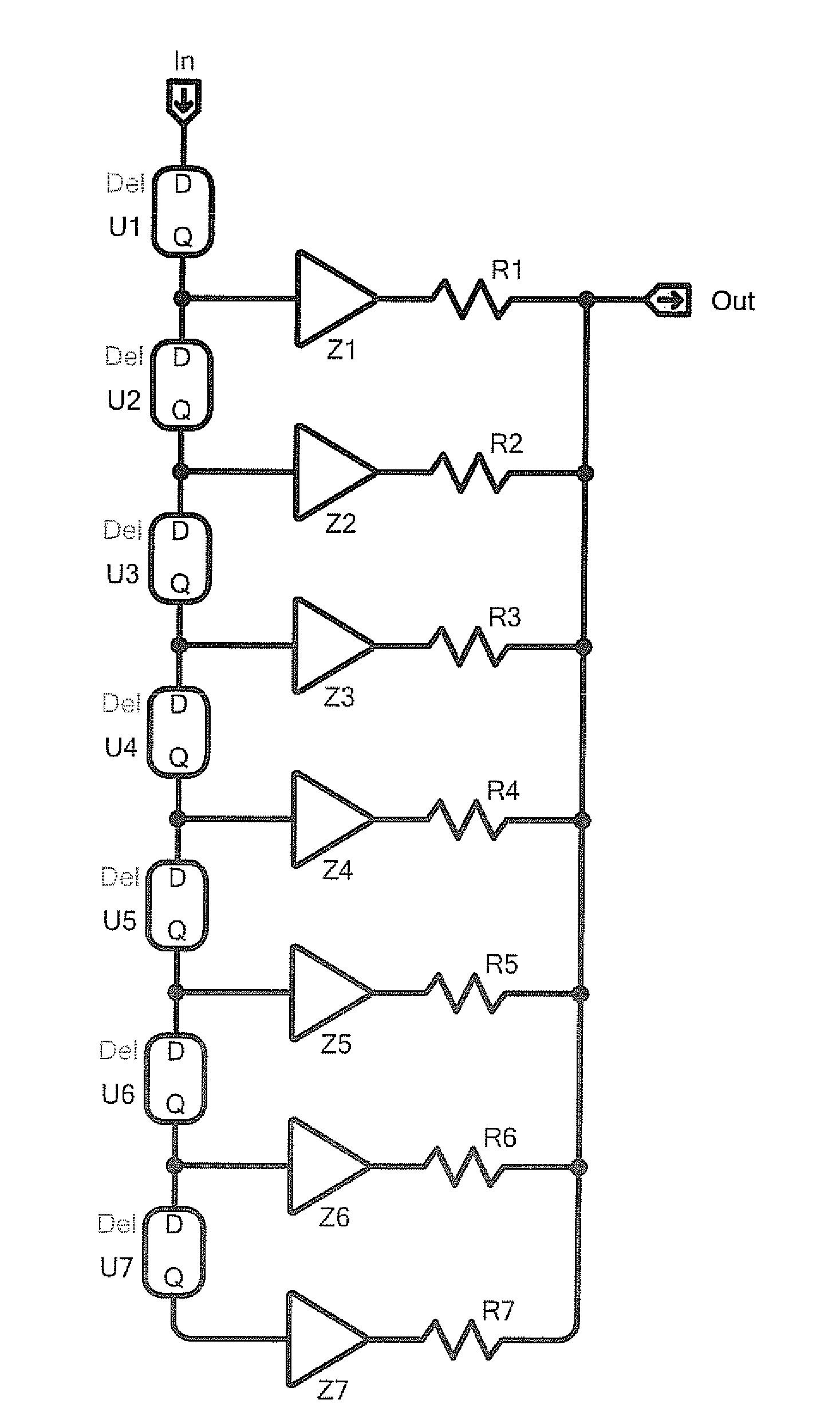
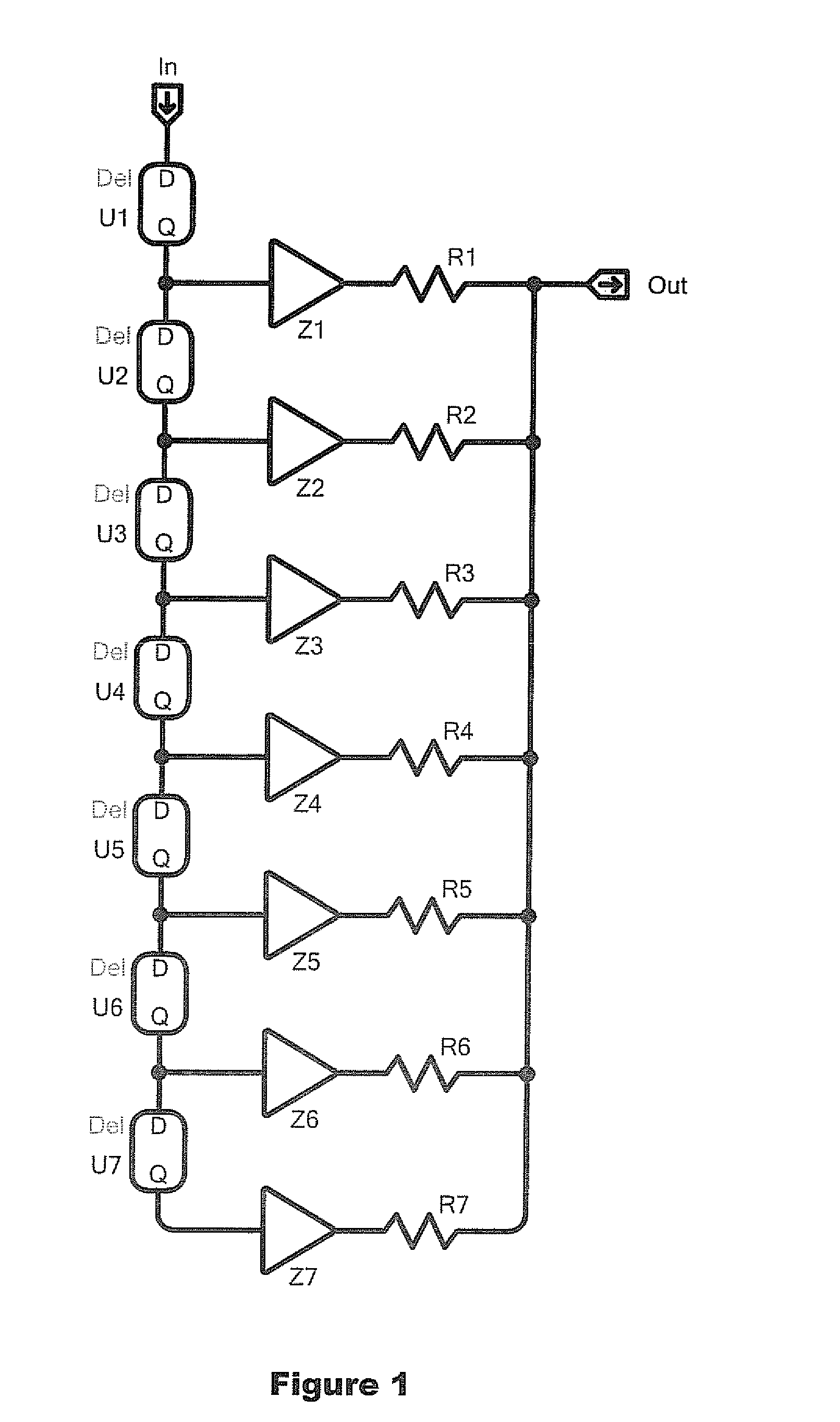
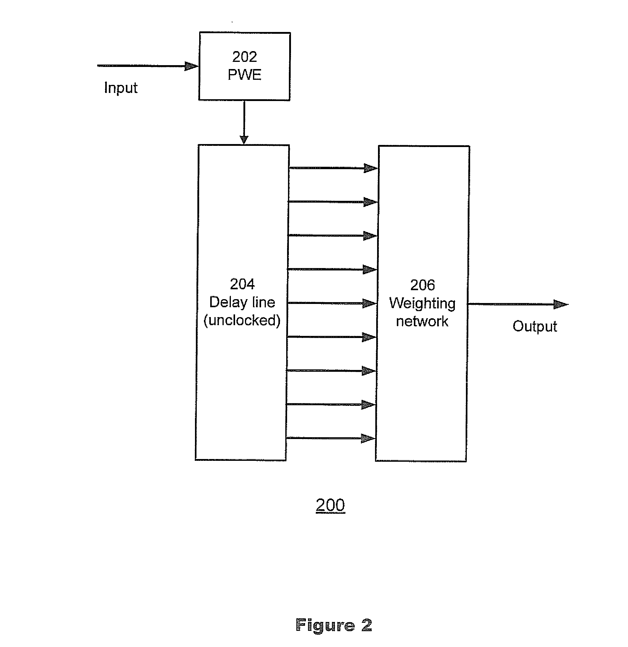
[0030]The present application describes a finite impulse response (FIR) filter using unclocked delay elements, rather than clocked analog delay elements. Like a conventional FIR filter, such a filter accepts an analog signal and produces an analog signal, but provides a simpler way of filtering certain analog signals than conventional filters.

[0031]The delay elements of a filter according to the present application are unclocked, such as logic gates which have a propagation delay but do not require or use clocking, rather than clocked delay elements such as DFFs or other clocked elements that are used in conventional FIR filters. The propagation of the input signal is thus due only to the delay inherent in each gate, and occurs based upon when a signal reaches the gate rather than being caused, by a clock signal.

[0032]The logic gates do not act as sampling devices as in a conventional FIR filter, and thus the input analog signal must be converted, to a digital signal before it is ap...


PUM


Abstract

A system and method for filtering an analog signal with a finite impulse response (FIR) filter that does not require analog delay elements are disclosed. An analog signal is pulse-width encoded, and the pulse-width encoded signal passed to a delay line comprising unclocked delay elements, such as logic gates, rather than clocked delay elements such as are used in conventional FIR filters. The propagation of the input signal is thus due only to the delay inherent in each gate, and occurs based upon when a signal reaches the gate rather than being caused by a clock signal. As with a conventional FIR filter, weighting elements having impedance are used to weigh the output of each delay element, and the resulting outputs summed to obtain a filtered output signal. For certain signals, such a circuit and method provides a simpler way of filtering than conventional filters.

Description

[0001]This application claims priority from Provisional Application No. 61 / 715,250, filed Oct. 17, 2012, which is incorporated by reference herein in its entirety.FIELD OF THE INVENTION[0002]The present invention relates generally to electronic filters, and more particularly to finite impulse response (FIR) filters.BACKGROUND OF THE INVENTION[0003]Analog filters having well-defined and steep transition bands (the range of frequencies where the filter goes from passing the signal to blocking the signal) can be complex and costly. The components of such filters may be hard to match, particularly on a single silicon chip because the transfer function, as represented in a pole-zero analysis, requires many poles and / or zeros which must all match. As the filler order increases, i.e., as more poles and zeros are required, the Q of the filter (the bandwidth relative to the center frequency) typically increases, and high-Q circuits require low noise and high dynamic range.[0004]Some such ana...

Claims


Application Information

Patent Timeline
IPC IPC(8): H04L25/49
CPCH04L25/4902H03H17/06H03H17/0213
Inventor MALLINSON, A. MARTIN
Owner ESS TECHNOLOGY
Why Eureka
Try Eureka