Semiconductor Packages with Integrated Antenna and Method of Forming Thereof

a technology of integrated antennas and semiconductors, applied in the field of semiconductor packages, can solve problems such as increasing the overall cos

Active Publication Date: 2014-04-24
INFINEON TECH AG
View PDF1 Cites 72 Cited by
  • Summary
  • Abstract
  • Description
  • Claims
  • Application Information

AI Technical Summary

Problems solved by technology

However, such construction increases the overall cost due to the ext

Method used


Image

  • Semiconductor Packages with Integrated Antenna and Method of Forming Thereof
  • Semiconductor Packages with Integrated Antenna and Method of Forming Thereof
  • Semiconductor Packages with Integrated Antenna and Method of Forming Thereof

Examples


Embodiment Construction

[0035]The making and using of various embodiments are discussed in detail below. It should be appreciated, however, that the present invention provides many applicable inventive concepts that can be embodied in a wide variety of specific contexts. The specific embodiments discussed are merely illustrative of specific ways to make and use the invention, and do not limit the scope of the invention.

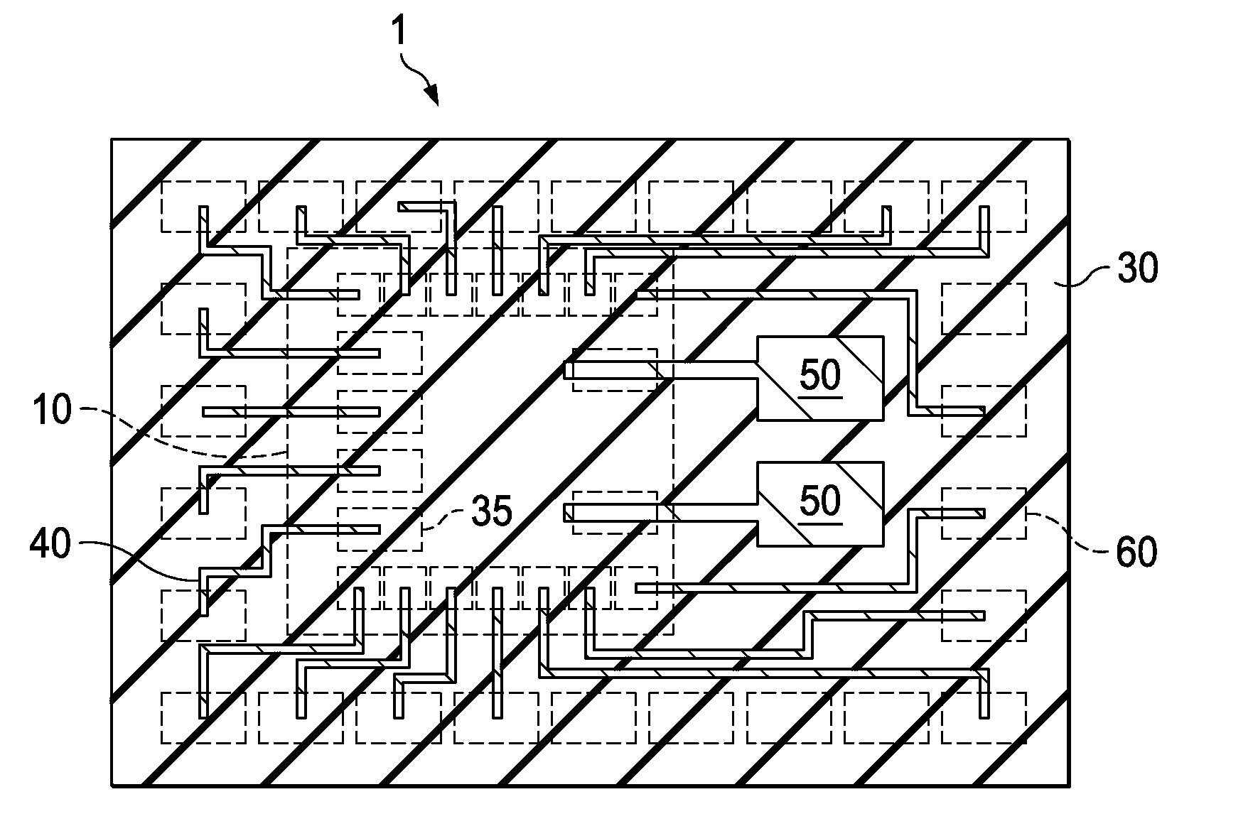
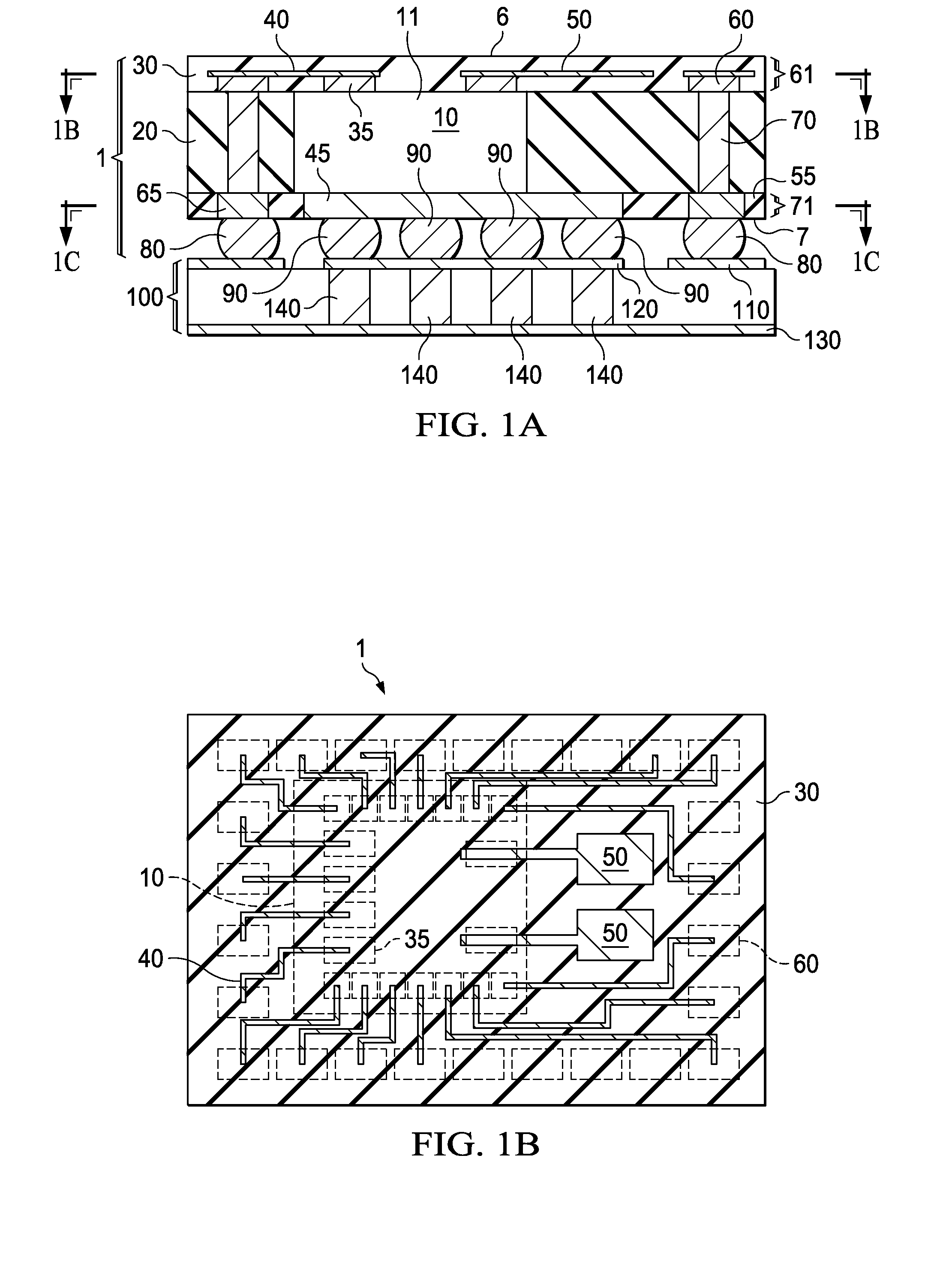
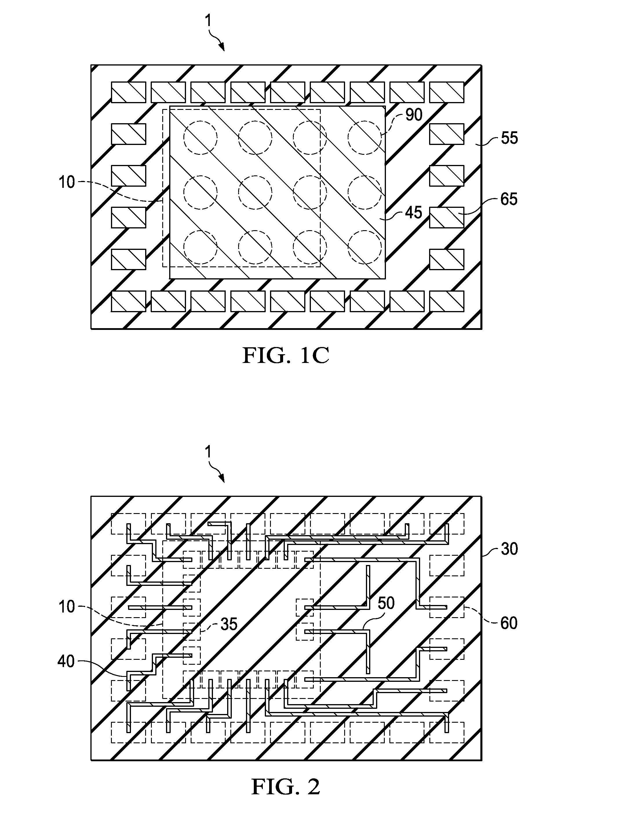
[0036]Conventional antennas integrated within a semiconductor package have many problems. In conventional antenna designs, the antenna is integrated in the fan-out area of semiconductor package. In such conventional antenna designs, a reflector is placed at the top surface of the printed circuit board below the antenna. Consequently, critical parameters of an antenna such as impedance matching, bandwidth, directional characteristic etc. strongly depend on the distance between the antenna and the printed circuit board (PCB). However, this distance is determined during the mounting of the semi...


PUM


Abstract

In one embodiment of the present invention, a semiconductor package includes a substrate having a first major surface and an opposite second major surface. A chip is disposed in the substrate. The chip includes a plurality of contact pads at the first major surface. A first antenna structure is disposed at the first major surface. A reflector is disposed at the second major surface.

Description

CROSS-REFERENCE TO RELATED APPLICATIONS[0001]The application relates to the following co-pending and commonly assigned patent applications: Ser. No. 13 / 736,097, filed Jan. 8, 2013; and Ser. No. ______, Attorney Docket No.: INF 2012 P 51103 US, filed Jan. 8, 2013, which applications are incorporated herein by reference.[0002]This application claims priority to European Patent Application 12007249.1, which was filed Oct. 19, 2012 and is incorporated herein by reference.TECHNICAL FIELD[0003]The present invention relates generally to semiconductor packages, and more particularly to semiconductor packages with integrated antenna and methods of forming thereof.BACKGROUND[0004]Recently, interest in the millimeter-wave spectrum at 10 GHz to 300 GHz has drastically increased. The emergence of low cost high performance CMOS technology has opened a new perspective for system designers and service providers because it enables the development of millimeter-wave radios at the same cost structure ...

Claims


Application Information

Patent Timeline
IPC IPC(8): H01L23/498H01L21/768
CPCH01L21/76885H01L23/49816H01L23/3128H01Q1/2283H01Q9/0407H01Q9/16H01Q23/00H01L23/49822H01L23/5389H01L2224/215H01L2224/211H01L24/19H01L24/20H01L2224/12105H01L2224/131H01L2224/16227H01L2224/16245H01L2224/82101H01L2224/96H01L21/568H01L2924/1301H01L2224/17519H01L2924/181H01L2924/12042H01L2223/6677H01L2224/16225H01L23/49827H01L2224/19H01L2924/014H01L2924/01022H01L2924/01074H01L2924/04941H01L2924/04953H01L2924/01029H01L2924/01055H01L2924/01064H01L2924/01044H01L2924/01042H01L2924/01015H01L2924/0105H01L2924/00012H01L2924/00H01L21/76802H01L2924/0002
Inventor WOJNOWSKI, MACIEJHARTNER, WALTERGEITNER, OTTMARBEER, GOTTFRIEDPRESSEL, KLAUSPOUR MOUSAVI, MEHRAN
Owner INFINEON TECH AG
Why Eureka
Try Eureka