Pseudo-8t nvsram cell with a charge-follower

a nvsram cell and charge-following technology, applied in the field of pseudo8 t nvsram cells, can solve the problems of unreliable cell operation and large size of 12t nvsram cells, and achieve the effect of reducing cell size by 20%

Inactive Publication Date: 2014-05-01
APLUS FLASH TECH
View PDF4 Cites 3 Cited by
  • Summary
  • Abstract
  • Description
  • Claims
  • Application Information

AI Technical Summary

Benefits of technology

[0008]The present invention discloses a 10T NVSRAM cell with a 6T SRAM cell coupled with a 4T Flash cell having one dedicated Flash-based Charger. In addition, a Pseudo-8T NVSRAM cell with a shared Flash-based Charger between two adjacent 8T NVSRAM cells to top and bottom in layout is also disclosed to further reduce cell size by 20%.

Problems solved by technology

But, one major disadvantage of the above 12T NVSRAM cell is the big cell size.
After a long P / E endurance cycle, the distance of the gap of ΔVt of Erase and Program Vt becomes smaller, thus the big cell size of 12T NVSRAM may result in unreliable cell operations, especially for low 1.2V VDD operation.

Method used


Image

  • Pseudo-8t nvsram cell with a charge-follower
  • Pseudo-8t nvsram cell with a charge-follower
  • Pseudo-8t nvsram cell with a charge-follower

Examples


Embodiment Construction

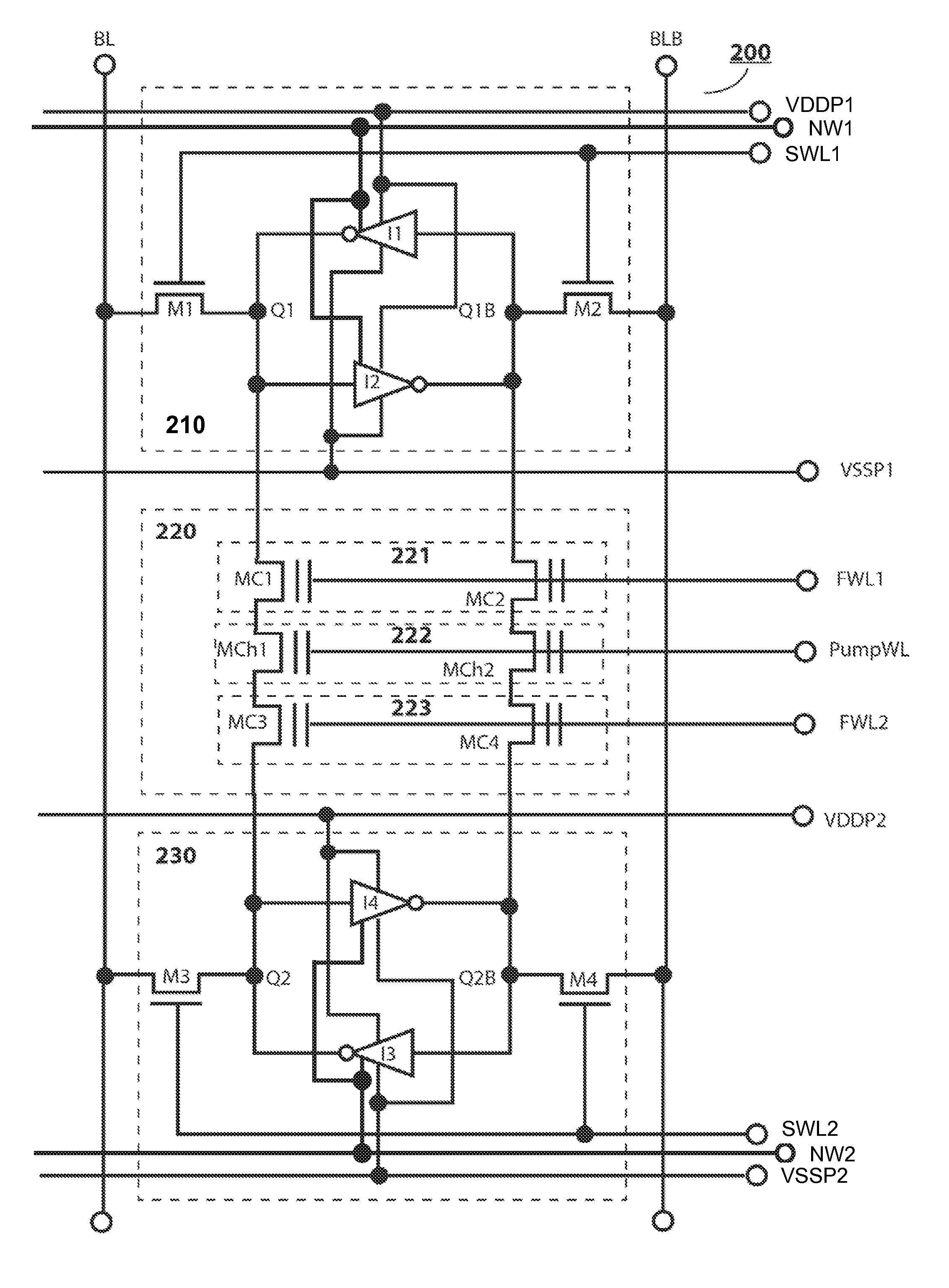
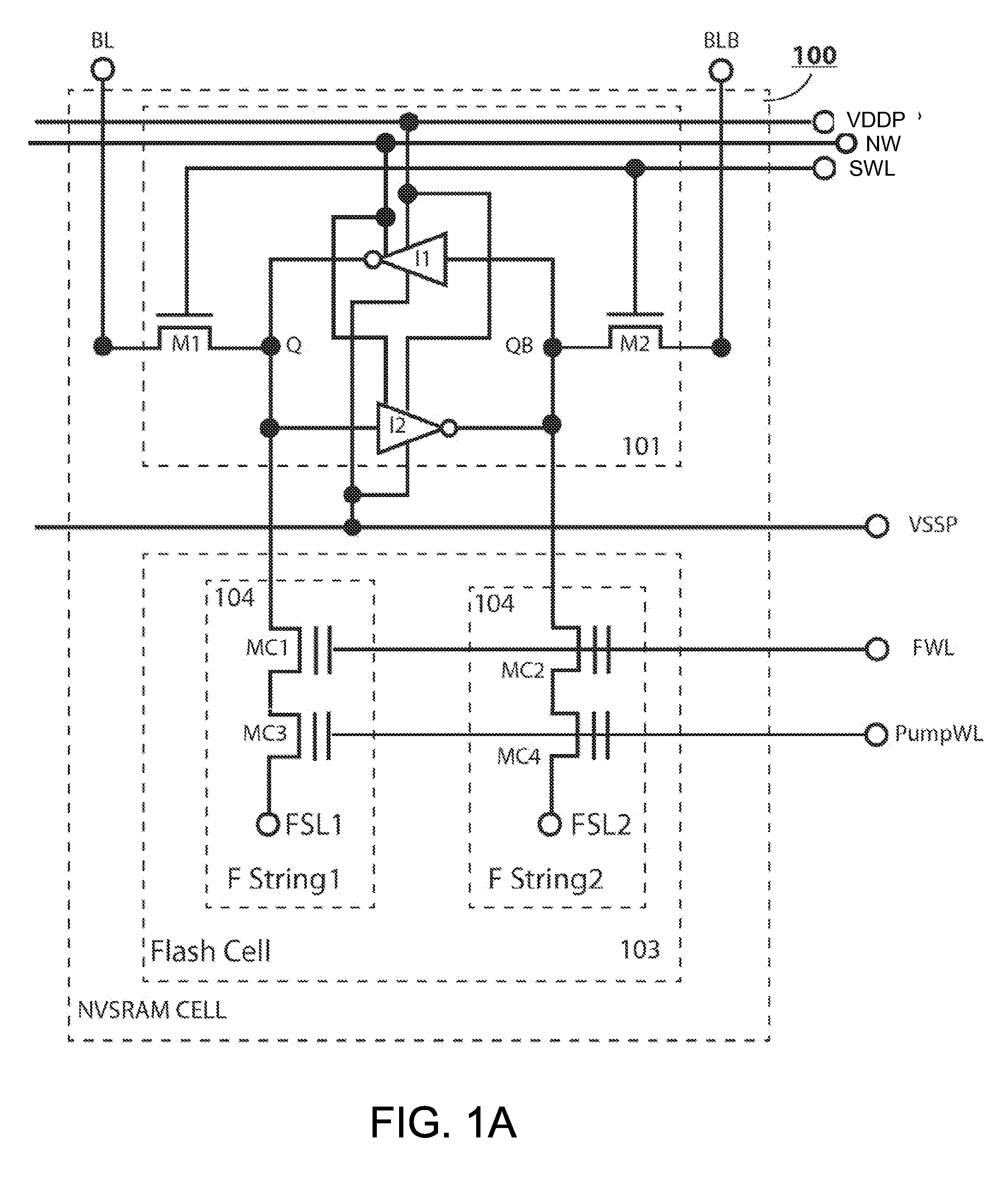
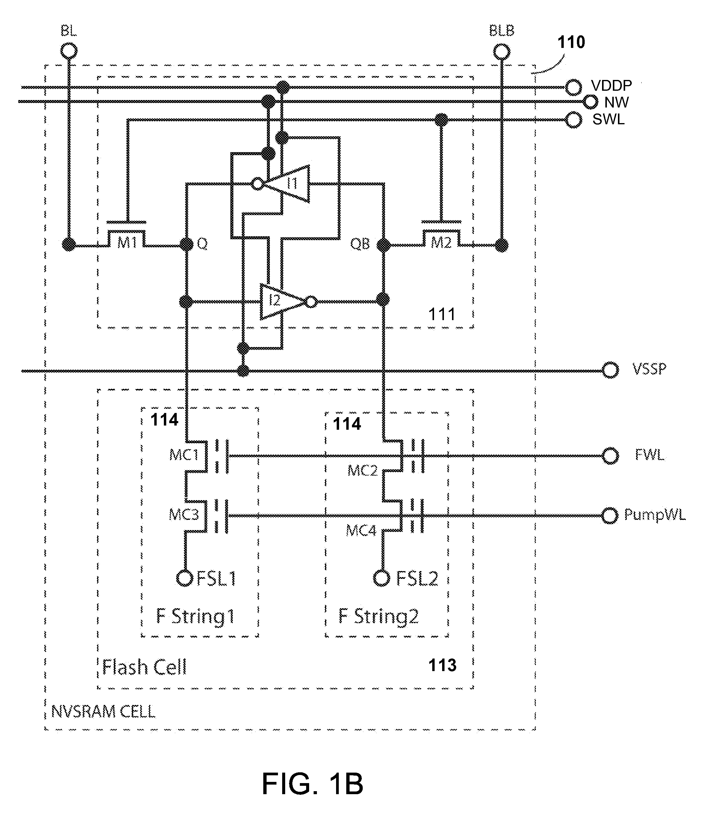
[0040]The present invention is related to improved cell architecture for NVSRAM memory device. Merely by example, the invention provides a 10-transistor (10T) NVSRAM cell with a flash Charger or a Pseudo-8T NVSRAM cell to reduce cell size from typical 12T NVSRAM cell. All key operations of the 10T NVSRAM cell with a flash Charger are provided under one or more operation schemes, no matter what the Flash cell within the NVSRAM cell is made by 1-poly SONOS or MONOS charge-trapping type, or 2-poly NMOS or PMOS floating-gate type.

[0041]FIG. 1A shows a first preferred embodiment of a 2-poly NMOS 10T NVSRAM cell with a flash Charger used for NVSRAM memory device of the present invention. The 10T NVSRAM cell 100 comprises one 6T LV SRAM cell 101 and one 4T NMOS 2-poly Flash cell 103. Each 4T NMOS 2-poly Flash cell comprises two fully symmetrical 2T NMOS 2-poly Flash strings, 104. Each String further comprises one 2-poly NMOS Flash transistor MC1 and one Flash-based Charger transistor, MC3,...


PUM


Abstract

The present invention discloses a 10T NVSRAM cell with a 6T SRAM cell with 4T Flash cell with one dedicated Flash-based Charger. In addition, a Pseudo-8T NVSRAM cell with a shared Flash-based Charger between two adjacent 8T NVSRAM cells at top and bottom in cell layout is also disclosed to further reduce cell size by 20%. As opposed to the prior art of 12T NVSRAM cell, the Store operation of the above two preferred embodiments use a DRAM-like charge-sensing scheme with Flash cell configured into a voltage follower ensured by the Flash-based Charger to obtain the final ΔVQ-QB>0.2V at Q and QB nodes of each SRAM cell to cover all the mismatched of parasitic capacitance in flash cell devices and layout for a reliable amplification by ramping up SRAM's VDD line and ramping down SRAM's VSS line.

Description

CROSS-REFERENCE TO RELATED APPLICATIONS[0001]This application claims priority to U.S. Patent Application No. 61 / 720,385, filed on Oct. 30, 2012, commonly assigned, and hereby incorporated by references in their entireties herein for all purposes.[0002]This application is related to U.S. Pat. No. 7,760,540, and U.S. patent application Ser. Nos. 14 / 037,356, 14 / 053,549, 14 / 058,227, and 14 / 059,618.TECHNICAL FIELD OF THE INVENTION[0003]The present invention relates to a preferred Pseudo-8T NVSRAM cell along with a Flash-based Charge-follower that takes a layout room of one flash row or of an active spacing between two adjacent Flash transistor source nodes in y-direction, thus no extra silicon area is required. Each Pseudo-8T NVSRAM cell further comprises one 6T LV SRAM cell and one 2T HV Flash cell in a paired 1T Flash string containing only one Flash transistor but with another one flash transistor used as a Charger for the HV supply of a Flash-based voltage follower in each individual...

Claims


Application Information

Patent Timeline
Patent Type & Authority Applications(United States)
IPC IPC(8): G11C14/00
CPCG11C14/0063
Inventor LEE, PETER WUNG
Owner APLUS FLASH TECH
Why Eureka
Try Eureka