Wiring substrate

a technology of wiring substrate and wire, which is applied in the direction of final product manufacturing, sustainable manufacturing/processing, and semiconductor/solid-state device details

Active Publication Date: 2014-05-08
NGK SPARK PLUG CO LTD
View PDF4 Cites 21 Cited by
  • Summary
  • Abstract
  • Description
  • Claims
  • Application Information

AI Technical Summary

Benefits of technology

[0014]As described above, the present invention can provide a wiring substrate configured to prevent the occurrence of a short circuit between the connection terminals and to implement a fine-pitch disposition of the connection terminals.

Problems solved by technology

However, in the case where a plurality of connection terminals are disposed at a fine pitch within the same opening, solder coated on the surface of a certain connection terminal may flow to an adjacent connection terminal, potentially resulting in the occurrence of a short circuit between the connection terminals.

Method used


Image

  • Wiring substrate
  • Wiring substrate
  • Wiring substrate

Examples


first embodiment

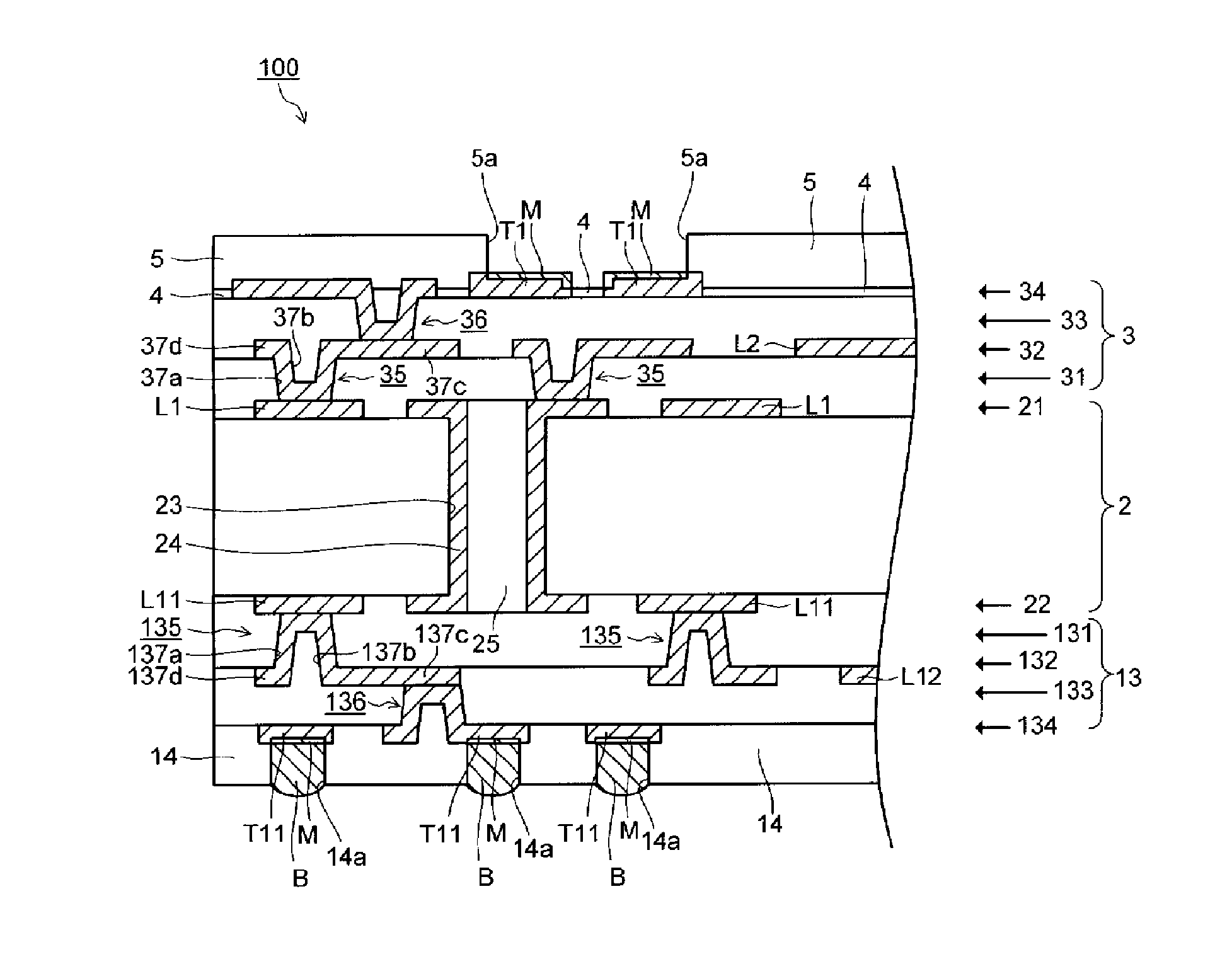
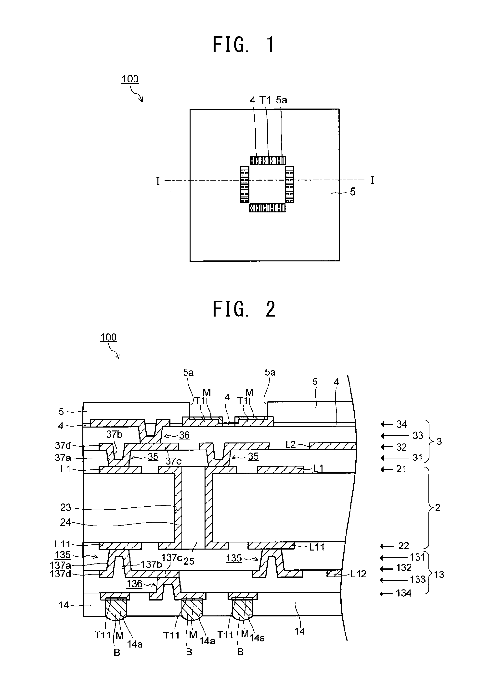
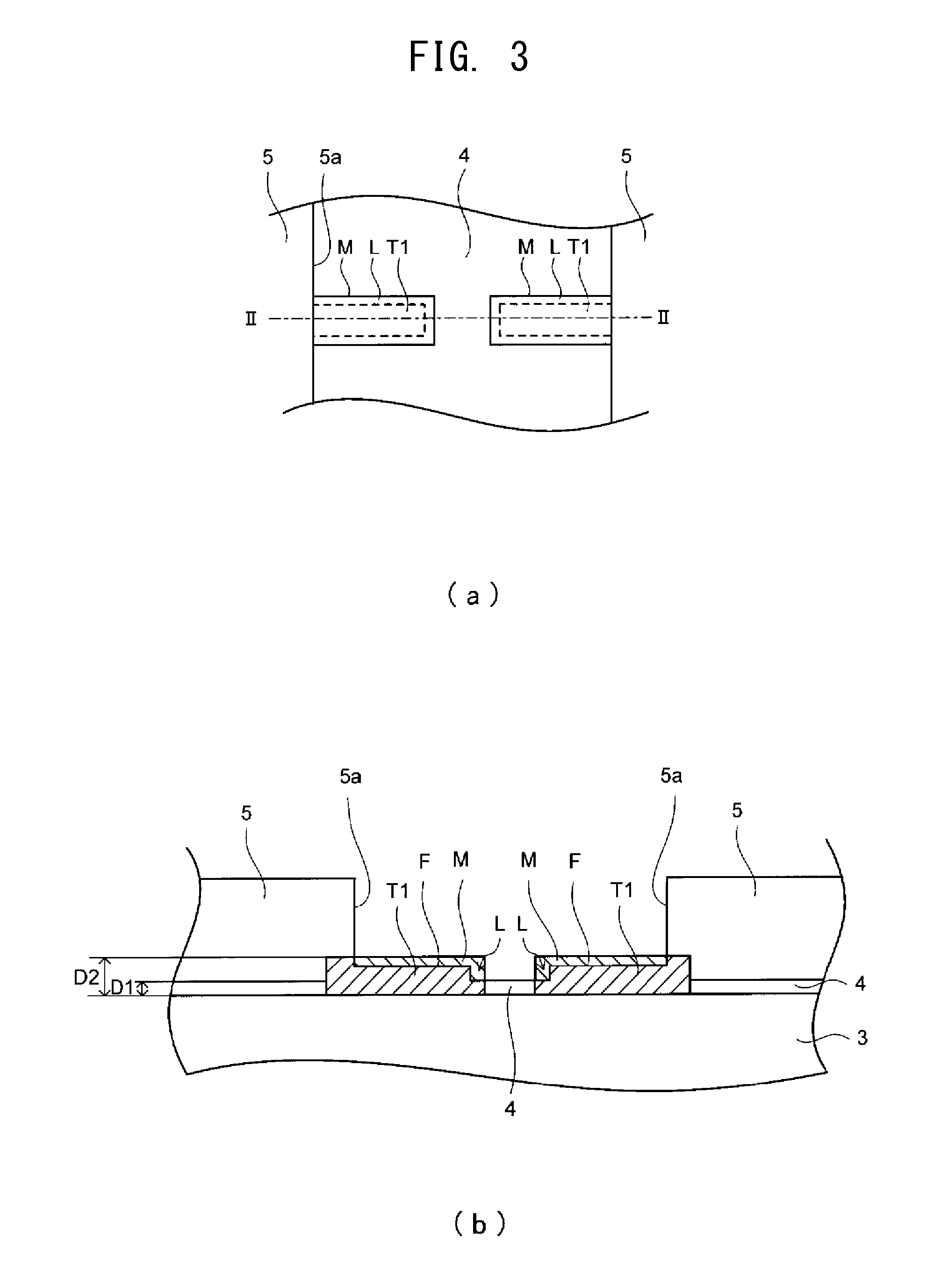
[0047]FIG. 1 is a plan view (front side) of a wiring substrate 100 according to a first embodiment. FIG. 2 is a fragmentary, sectional view of the wiring substrate 100 taken along line I-I of FIG. 1. FIG. 3 is a pair of configurational views of connection terminals T1 formed on the front side of the wiring substrate 100. FIG. 3(a) is a top view of the connection terminals T1. FIG. 3(b) is a sectional view taken along line II-II of FIG. 3(a). In the following description, a side of the wiring substrate 100 on which a semiconductor chip is connected is referred to as the front side, and a side on which a motherboard, a socket, or the like (hereinafter, referred to as a motherboard or the like) is connected is referred to as the back side.

(Configuration of the Wiring Substrate 100)

[0048]The wiring substrate 100 shown in FIGS. 1 to 3 includes a core substrate 2; a build-up layer 3 (front side) on which a plurality of the connection terminals T1 are formed for connection to a semiconduct...

second embodiment

[0085]FIG. 12 is a plan view (front side) of a wiring substrate 200 according to a second embodiment. FIG. 13 is a fragmentary, sectional view of the wiring substrate 200 taken along line I-I of FIG. 12. FIG. 14 is a pair of configurational views of connection terminals T2 formed on the front side of the wiring substrate 200. FIG. 14(a) is a top view of the connection terminals T2. FIG. 14(b) is a sectional view taken along line II-II of FIG. 14(a). The configuration of the wiring substrate 200 will next be described with reference to FIGS. 12 to 14; however, configurational features similar to those of the wiring substrate 100 described above with reference to FIGS. 1 to 3 are denoted by like reference numerals, and repeated description thereof is omitted.

(Configuration on the Front Side)

[0086]On the front side of the wiring substrate 200, a cover plating layer 41 electrically connected to the core conductive-layer 21 is formed, and the cover plating layer 41 and the conductive lay...

third embodiment

[0093]FIG. 15 is a plan view (front side) of a wiring substrate 300 according to a third embodiment. FIG. 16 is a fragmentary, sectional view of the wiring substrate 300 taken along line I-I of FIG. 15. FIG. 17 is a pair of configurational views of connection terminals T3 formed on the front side of the wiring substrate 300. FIG. 17(a) is a top view of the connection terminals T3. FIG. 17(b) is a sectional view taken along line II-II of FIG. 17(a).

[0094]The wiring substrate 300 according to the third embodiment differ from the wiring substrate 200 described above with reference to FIGS. 12 to 14 in that the connection terminals T3 and T11 are formed directly on the conductive layers 32 and 132, respectively, without involvement of vias. The configuration of the wiring substrate 300 will next be described with reference to FIGS. 15 to 17; however, configurational features similar to those of the wiring substrate 100 described above with reference to FIGS. 1 to 3 and the wiring substr...


PUM


Abstract

A wiring substrate according to the present invention includes a laminate of one or more insulation layers and one or more conductive layers and further includes a plurality of connection terminals formed on the laminate and spaced apart from one another, each having a step formed at the outer periphery of a first main surface opposite a contact surface in contact with the laminate, and a filling member provided in a filling manner between the connection terminals.

Description

TECHNICAL FIELD[0001]The present invention relates to a wiring substrate having a plurality of connection terminals formed on its main surface for connection to a semiconductor chip.BACKGROUND ART[0002]Usually, a wiring substrate has terminals formed on its main surface (front surface) for connection to a semiconductor chip (hereinafter referred to as connection terminals). In recent years, the disposition density of the connection terminals has been increasing; accordingly, the pitch between the connection terminals to be disposed has become finer. Thus, there is proposed a wiring substrate which employs the NSMD (non solder mask defined) feature in which a plurality of connection terminals are disposed within the same opening.[0003]However, in the case where a plurality of connection terminals are disposed at a fine pitch within the same opening, solder coated on the surface of a certain connection terminal may flow to an adjacent connection terminal, potentially resulting in the ...

Claims


Application Information

Patent Timeline
Patent Type & Authority Applications(United States)
IPC IPC(8): H05K1/02
CPCH05K1/0213H05K1/111H05K3/3436H05K3/3452H05K3/4661H05K2201/09918H05K3/4007H05K2201/0195H05K2201/09881H05K2201/099H01L23/145H01L23/49816H01L23/49822H01L23/49827H01L23/49894H01L2924/0002Y02P70/50H01L2924/00H05K3/34H05K3/28H05K3/38H05K3/46
Inventor ITO, TATSUYAMORI, SEIJIHAYASHI, TAKAHIROWAKAZONO, MAKOTONISHIDA, TOMOHIRO
Owner NGK SPARK PLUG CO LTD
Why Eureka
Try Eureka