Solid-state image sensor, method of manufacturing the same and camera

a technology of solid-state image sensor and manufacturing method, which is applied in the direction of color television, color television, television system scanning details, etc., can solve problems such as color mixing, and achieve the effect of reducing color mixing

Inactive Publication Date: 2014-05-15
CANON KK
View PDF7 Cites 28 Cited by
  • Summary
  • Abstract
  • Description
  • Claims
  • Application Information

AI Technical Summary

Benefits of technology

[0006]The present invention provides a tech

Problems solved by technology

In this case, light which should be detected in the first pixel is

Method used


Image

  • Solid-state image sensor, method of manufacturing the same and camera
  • Solid-state image sensor, method of manufacturing the same and camera
  • Solid-state image sensor, method of manufacturing the same and camera

Examples


first embodiment

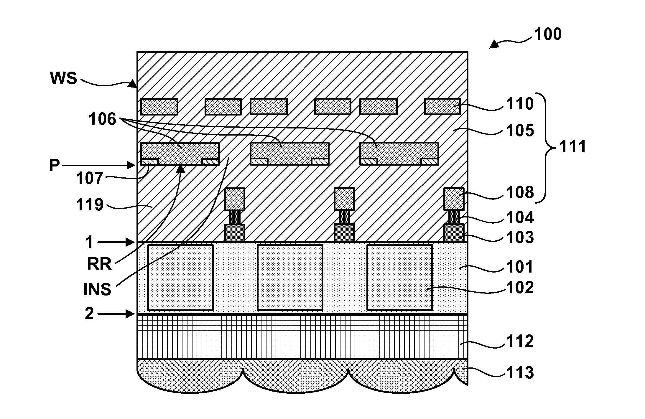
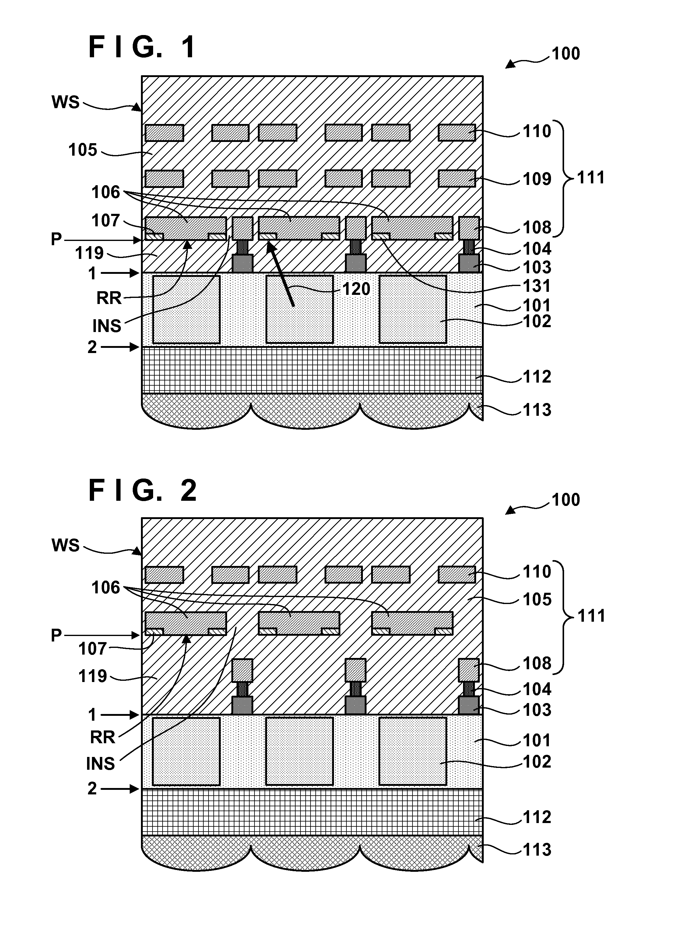
[0024]FIG. 1 schematically shows the sectional structure of a solid-state image sensor 100 according to the present invention. Note that FIG. 1 shows only three pixels but the solid-state image sensor 100 can include a larger number of pixels. The solid-state image sensor 100 can include a semiconductor layer 101 having a first face 1 and second face 2, a plurality of photoelectric converters 102 two-dimensionally arranged in the semiconductor layer 101, and a wiring structure WS arranged on the side of the first face 1. The solid-state image sensor 100 is configured so that light from an object is incident on the second face 2 through an imaging lens. That is, the solid-state image sensor 100 is formed as a back-side illumination solid-state image sensor in which a wiring structure is arranged on the side of the first face of a semiconductor layer and light from an object is incident on the second face of the semiconductor layer. A plurality of microlenses 113 can be typically arra...

second embodiment

[0047]In the second embodiment, it is possible to improve the degree of freedom of wiring by forming each reflection portion 106 as part of a wiring pattern for communicating an electric signal. Each reflection portion 106 may be formed as part of a wiring pattern for communicating an electric signal in a wiring layer other than a wiring layer 108 of a first layer, for example, a wiring layer 109 of a second layer or a wiring layer 110 of a third layer.

[0048]A solid-state image sensor 100 according to the third embodiment of the present invention will be described below with reference to FIGS. 6A and 6B. Note that points not mentioned in the third embodiment can comply with at least one of the first and second embodiments.

[0049]A plurality of photoelectric converters 102 include a first photoelectric converter 102 on which light of a first wavelength range is incident, a second photoelectric converter 102 on which light of a second wavelength range is incident, and a third photoelec...

third embodiment

[0052]The third embodiment is useful when the layouts of a plurality of pixels are different from each other, and it is difficult to provide reflection portions 106 and light absorbing portions 107 in all the pixels, for example, when a plurality of photoelectric converters 102 share a floating diffusion.

[0053]A solid-state image sensor 100 according to the fourth embodiment of the present invention will be described below with reference to FIGS. 7 to 11B. Note that points not mentioned in the fourth embodiment can comply with at least one of the first to third embodiments. In the solid-state image sensor 100 according to the fourth embodiment, the relative position between a photoelectric converter 102 and a corresponding reflection region RR and light absorbing portion 107 is determined depending on the position of the photoelectric converter 102 in a semiconductor layer 101.

[0054]When the position of the photoelectric converter 102 in the semiconductor layer 101 changes, the dire...


PUM


Abstract

An image sensor includes a semiconductor layer having first and second faces, and a wiring structure arranged on a side of the first face, wherein photoelectric converters are arranged in the semiconductor layer and light is incident on the second face. The wiring structure includes reflection portions having reflection regions and arranged for at least some of the photoelectric converters, absorbing portions arranged around the reflection regions, an insulator portion arranged to surround the absorbing portions, and an interlayer insulating film arranged between the first face and a group of the reflection portions, the light absorbing portions, and the insulator portion, and a reflectance of the light absorbing portions is smaller than a reflectance of the reflection regions, and a light transmittance of the light absorbing portions is smaller than a light transmittance of the insulator portion.

Description

BACKGROUND OF THE INVENTION[0001]1. Field of the Invention[0002]The present invention relates to a solid-state image sensor, a method of manufacturing the same, and a camera.[0003]2. Description of the Related Art[0004]It has been required to improve the sensitivity of a solid-state image sensor used in a digital video camera, digital still camera, and the like. Japanese Patent Laid-Open No. 2011-151420 discloses a so-called back-side illumination solid-state image sensor. In the back-side illumination solid-state image sensor, if a semiconductor layer has a thickness of, for example, several μm or smaller, long-wavelength components of incident light having passed through a microlens pass through the semiconductor layer without being sufficiently absorbed. According to Japanese Patent Laid-Open No. 2011-151420, a reflection layer for returning, to the semiconductor layer, light having passed through the semiconductor layer is provided on the whole surface on the wiring layer side o...

Claims


Application Information

Patent Timeline
IPC IPC(8): H01L31/0232H04N5/369H01L31/18
CPCH01L31/0232H04N5/369H01L31/18H01L27/14621H01L27/14623H01L27/14627H01L27/14629H01L27/1464H01L27/14685H01L27/14636
Inventor SODA, TAKEHIKO
Owner CANON KK
Why Eureka
Try Eureka